NB7L111MMNG ON Semiconductor, NB7L111MMNG Datasheet - Page 4
NB7L111MMNG
Manufacturer Part Number
NB7L111MMNG
Description
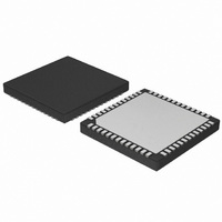
IC DRVR CLK/DATA 1:10 DIFF 52QFN
Manufacturer
ON Semiconductor
Type
Fanout Buffer (Distribution), Multiplexer , Datar
Datasheet
1.NB7L111MMNR2G.pdf
(13 pages)
Specifications of NB7L111MMNG
Number Of Circuits
1
Ratio - Input:output
2:10
Differential - Input:output
Yes/Yes
Input
CML, LVCMOS, LVDS, LVNECL, LVPECL, LVTTL
Output
CML
Frequency - Max
5.5GHz
Voltage - Supply
2.375 V ~ 3.465 V
Operating Temperature
-40°C ~ 85°C
Mounting Type
Surface Mount
Package / Case
52-VFQFN Exposed Pad
Frequency-max
5.5GHz
Output Logic Level
CML
Supply Voltage (max)
3.465 V
Supply Voltage (min)
2.375 V
Maximum Operating Temperature
+ 85 C
Maximum Data Rate
6 Gbps
Minimum Operating Temperature
- 40 C
Mounting Style
SMD/SMT
Number Of Clock Inputs
2
Supply Current
290 mA
Lead Free Status / RoHS Status
Lead free / RoHS Compliant
Available stocks
Company
Part Number
Manufacturer
Quantity
Price
Company:

Part Number:
NB7L111MMNG
Manufacturer:
ON Semiconductor
Quantity:
15
Part Number:
NB7L111MMNG
Manufacturer:
ON/安森美
Quantity:
20 000


Stresses exceeding Maximum Ratings may damage the device. Maximum Ratings are stress ratings only. Functional operation above the
Recommended Operating Conditions is not implied. Extended exposure to stresses above the Recommended Operating Conditions may affect
device reliability.
4. Maximum Ratings are those values beyond which device damage may occur.
5. JEDEC standard multilayer board − 1S2P (1 signal, 2 power).
Table 4. MAXIMUM RATINGS
Symbol
V
V
V
I
I
T
T
q
q
T
in
out
A
stg
JA
JC
sol
CC
I
INPP
Positive Power Supply
Input Voltage
Differential Input Voltage |CLK − CLK|
Input Current Through R
Output Current
Operating Temperature Range
Storage Temperature Range
Thermal Resistance (Junction−to−Ambient)
(Note 5)
Thermal Resistance (Junction−to−Case)
Wave Solder
Table 3. ATTRIBUTES
3. For additional information, see Application Note AND8003/D.
Input Default State Resistors
ESD Protection
Moisture Sensitivity (Note 3)
Flammability Rating
Transistor Count
Meets or exceeds JEDEC Spec EIA/JESD78 IC Latchup Test
Parameter
(Note 4)
T
(50 W Resistor)
Characteristics
Pb−Free
Pb
http://onsemi.com
Oxygen Index: 28 to 34
V
V
V
V
Continuous
Surge
Continuous
Surge
QFN52
0 lfpm
500 lfpm
1S2P (Note 8)
EE
EE
CC
CC
Human Body Model
Condition 1
= 0 V
= 0 V
− V
− V
Machine Model
4
EE
EE
≥ 2.8 V
< 2.8 V
QFN−52
R1, R3
R2
V
QFN52
QFN52
EE
Condition 2
v V
Pb Pkg
Level 2
UL 94 V−0 @ 0.125 in
I
v V
> 1400 V
> 80 V
Value
56 kW
75 kW
CC
339
Pb−Free Pkg
Level 1
−65 to +150
|V
−40 to +85
CC
Rating
19.6
265
265
3.6
3.6
2.8
25
50
25
50
25
21
− V
EE
|
°C/W
°C/W
°C/W
Unit
mA
mA
mA
mA
°C
°C
°C
V
V
V
V
Related parts for NB7L111MMNG
Image
Part Number
Description
Manufacturer
Datasheet
Request
R

Part Number:
Description:
ON Semiconductor [VOLTAGE REGULATOR]
Manufacturer:
ON Semiconductor
Datasheet:
Part Number:
Description:
357-036-542-201 CARDEDGE 36POS DL .156 BLK LOPRO
Manufacturer:
ON Semiconductor
Datasheet:
Part Number:
Description:
357-036-542-201 CARDEDGE 36POS DL .156 BLK LOPRO
Manufacturer:
ON Semiconductor
Datasheet:
Part Number:
Description:
357-036-542-201 CARDEDGE 36POS DL .156 BLK LOPRO
Manufacturer:
ON Semiconductor
Datasheet:
Part Number:
Description:
357-036-542-201 CARDEDGE 36POS DL .156 BLK LOPRO
Manufacturer:
ON Semiconductor
Datasheet:
Part Number:
Description:
357-036-542-201 CARDEDGE 36POS DL .156 BLK LOPRO
Manufacturer:
ON Semiconductor
Datasheet:
Part Number:
Description:
357-036-542-201 CARDEDGE 36POS DL .156 BLK LOPRO
Manufacturer:
ON Semiconductor
Datasheet:
Part Number:
Description:
357-036-542-201 CARDEDGE 36POS DL .156 BLK LOPRO
Manufacturer:
ON Semiconductor
Datasheet:
Part Number:
Description:
357-036-542-201 CARDEDGE 36POS DL .156 BLK LOPRO
Manufacturer:
ON Semiconductor
Datasheet:
Part Number:
Description:
357-036-542-201 CARDEDGE 36POS DL .156 BLK LOPRO
Manufacturer:
ON Semiconductor
Datasheet:
Part Number:
Description:
357-036-542-201 CARDEDGE 36POS DL .156 BLK LOPRO
Manufacturer:
ON Semiconductor
Datasheet:
Part Number:
Description:
Manufacturer:
ON Semiconductor
Datasheet:
Part Number:
Description:
Manufacturer:
ON Semiconductor
Datasheet:
Part Number:
Description:
Manufacturer:
ON Semiconductor
Datasheet: