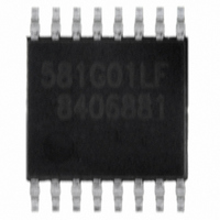
ICS581G-01LF IDT, Integrated Device Technology Inc, ICS581G-01LF Datasheet - Page 3

ICS581G-01LF
Manufacturer Part Number
ICS581G-01LF
Description
IC CLK MUX ZD GLITCHFREE 16TSSOP
Manufacturer
IDT, Integrated Device Technology Inc
Series
ClockBlocks™r
Type
Fanout Distribution, Multiplexer , Zero Delay Bufferr
Specifications of ICS581G-01LF
Pll
Yes
Input
Clock
Output
Clock
Number Of Circuits
1
Ratio - Input:output
2:4
Differential - Input:output
No/No
Frequency - Max
200MHz
Divider/multiplier
Yes/No
Voltage - Supply
3 V ~ 5.5 V
Operating Temperature
0°C ~ 70°C
Mounting Type
Surface Mount
Package / Case
16-TSSOP
Frequency-max
200MHz
Number Of Elements
1
Pll Input Freq (min)
6MHz
Pll Input Freq (max)
200MHz
Operating Supply Voltage (typ)
3.3V
Operating Temp Range
0C to 70C
Package Type
TSSOP
Operating Supply Voltage (min)
3V
Operating Supply Voltage (max)
5.5V
Operating Temperature Classification
Commercial
Pin Count
16
Lead Free Status / RoHS Status
Lead free / RoHS Compliant
Other names
581G-01LF
800-1080
800-1080-5
800-1080
800-1080
800-1080-5
800-1080
Available stocks
Company
Part Number
Manufacturer
Quantity
Price
Company:
Part Number:
ICS581G-01LF
Manufacturer:
IDT Integrated Device Technolo
Quantity:
135
Company:
Part Number:
ICS581G-01LF
Manufacturer:
IDT
Quantity:
264
Part Number:
ICS581G-01LF
Manufacturer:
IDT
Quantity:
20 000
Pin Descriptions
Device Operation
The ICS581-01 and ICS581-02 are very similar. Following is
a description of the operation of the ICS581-01 and the
differences of the ICS581-02.
The ICS581-01 is a PLL-based, zero delay, clock
multiplexer. The device consists of an input multiplexer
controlled by SELA that selects between two clock inputs.
The output of the mux drives the reference input of a phase
locked loop. The other input to the PLL comes from a
feedback input pin called FBIN. The output of the PLL drives
four low skew outputs. These chip outputs are therefore
buffered versions of the selected input clock with zero delay
and 50/50 duty cycle.
For correct operation, one of the clock outputs must be
connected to FBIN. In this datasheet, CLK4 is shown as the
feedback, but any one of the four clock outputs can be used.
If output termination resistors are used, the feedback should
be connected before the resistor. It is a property of the PLL
used on this chip that it will align rising edges on FBIN and
IDT™ / ICS™ ZERO DELAY GLITCH-FREE CLOCK MULTIPLEXER
ICS581-01/02
ZERO DELAY GLITCH-FREE CLOCK MULTIPLEXER
Number
16 (-01)
16 (-02)
Pin
10
11
12
13
14
15
1
2
3
4
5
6
7
8
9
Name
SELA
CLK4
CLK3
CLK2
CLK1
FBIN
GND
GND
VDD
OE0
OE1
VDD
Pin
INA
INB
DIV
S0
S1
Output
Output
Output
Output
Power
Power
Power
Power
Type
Input
Input
Input
Input
Input
Input
Input
Input
Input
Pin
Select 0 for frequency range. See table. Internal pull-up.
Select 1 for frequency range. See table. Internal pull-up.
Power Supply. Connect to +3.3 V or +5 V.
Input Clock A.
Input Clock B.
Connect to ground.
Feedback input. Connect to a clock output.
Output enable 0. See table. Internal pull-up.
Output enable 1. See table. Internal pull-up.
Connect to ground.
Low skew clock output.
Low skew clock output.
Low skew clock output.
Low skew clock output.
Power Supply. Connect to +3.3 V or +5 V.
Mux select. Selects INA when high. Internal pull-up.
Timeout select. See table. Internal pull-up.
3
either INA or INB (depending on SELA). Since FBIN is
connected to a clock output, this means that the outputs
appear to align with the input with zero delay.
When the input select (SELA) is changed, the output clock
will change frequency and/or phase until it lines up with the
new input clock. This occurs in a smooth, gradual manner
without any short pulses or glitches and will typically take a
few tens of microseconds.
The part must be configured to operate in the correct
frequency range. The table on page two gives the
recommended range.
The four low skew outputs are controlled by two output
enable pins that allow either one, three, or four simultaneous
outputs. If both OE pins are low, the PLL is powered down.
Note that the clock driving the FBIN pin must not be
tri-stated unless the PLL is powered down. Otherwise the
Pin Description
ZDB AND MULTIPLEXER
ICS581-01/02
REV L 051310


