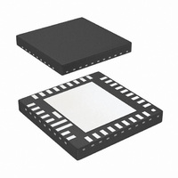
LMX2531LQE1226E/NOPB National Semiconductor, LMX2531LQE1226E/NOPB Datasheet - Page 25

LMX2531LQE1226E/NOPB
Manufacturer Part Number
LMX2531LQE1226E/NOPB
Description
IC PLL FREQ SYNTH W/VCO 36-LLP
Manufacturer
National Semiconductor
Series
PowerWise®r
Type
Clock/Frequency Synthesizer (RF)r
Datasheet
1.LMX2531LQ1778ENOPB.pdf
(36 pages)
Specifications of LMX2531LQE1226E/NOPB
Pll
Yes
Input
Clock
Output
CMOS
Number Of Circuits
1
Ratio - Input:output
2:2
Differential - Input:output
No/No
Frequency - Max
1.268GHz
Divider/multiplier
Yes/No
Voltage - Supply
2.8 V ~ 3.2 V
Operating Temperature
-40°C ~ 85°C
Mounting Type
Surface Mount
Package / Case
36-LLP
Frequency-max
1.268GHz
For Use With
LMX25311226EVAL - BOARD EVAL FOR LMX25311226
Lead Free Status / RoHS Status
Lead free / RoHS Compliant
Other names
LMX2531LQE1226ETR
2.4 REGISTER R3
2.4.1 DEN[21:12] -- Extension for the Fractional Denominator
These are the MSB bits of the DEN word, which have already been discussed.
2.4.2 FoLD[3:0] -- Multiplexed Output for Ftest/LD Pin
The FoLD[3:0] word is used to program the output of the Ftest/LD Pin. This pin can be used for a general purpose I/O pin, a lock
detect pin, and for diagnostic purposes. When programmed to the digital lock detect state, the output of the Ftest/LD pin will be
high when the part is in lock, and low otherwise. Lock is determined by comparing the input phases to the phase detector. The
analog lock detect modes put out a high signal with very fast negative pulses, that correspond to when the charge pump comes
on. This output can be low pass filtered with an RC filter in order to determine the lock detect state. If the open drain state is used,
a additional pull-up resistor is required. For diagnostic purposes, the options that allow one to view the output of the R counter or
the N counter can be very useful. Be aware that the output voltage level of the Ftest/LD is not equal to the supply voltage of the
part, but rather is given by V
2.4.3 ORDER -- Order of Delta Sigma Modulator
This bit determines the order of the delta sigma modulator in the PLL. In general, higher order fractional modulators tend to reduce
the primary fractional spurs that occur at increments of the channel spacing, but can also create spurs that are at a fraction of the
channel spacing, if there is not sufficient filtering. The optimal choice of modulator order is very application specific, however, a
third order modulator is a good starting point if not sure what to try first.
FoLD
10
11
12
13
14
15
0
1
2
3
4
5
6
7
8
9
OH
and V
ORDER
OL
in the electrical characteristics specification.
0
1
2
3
High Impedance
Output Type
Open-Drain
Push-Pull
Push-Pull
Push-Pull
Push-Pull
Push-Pull
Push-Pull
N/A
N/A
N/A
N/A
N/A
N/A
N/A
N/A
(Integer Mode - all fractions are ignored)
25
Delta Sigma Modulator Order
Reset Modulator
Second
Fourth
Third
N Counter Output Divided by 2
Analog Lock Detect
Analog Lock Detect
Digital Lock Detect
Logical High State
Logical Low State
R Counter Output
Reserved
Reserved
Reserved
Reserved
Reserved
Reserved
Reserved
Reserved
Function
Disabled
www.national.com


