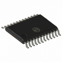
SI4136-F-GT Silicon Laboratories Inc, SI4136-F-GT Datasheet - Page 18

SI4136-F-GT
Manufacturer Part Number
SI4136-F-GT
Description
IC WLAN SAT RADIO 24TSSOP
Manufacturer
Silicon Laboratories Inc
Type
Frequency Synthesizerr
Datasheet
1.SI4126-F-GM.pdf
(34 pages)
Specifications of SI4136-F-GT
Package / Case
24-TSSOP
Pll
Yes
Input
Clock
Output
Clock
Number Of Circuits
1
Ratio - Input:output
1:2
Differential - Input:output
No/No
Frequency - Max
2.5GHz
Divider/multiplier
Yes/No
Voltage - Supply
2.7 V ~ 3.6 V
Operating Temperature
-40°C ~ 85°C
Mounting Type
Surface Mount
Frequency-max
2.5GHz
Operating Frequency
62.5 MHz to 1000 MHz
Supply Current
25.7 mA
Operating Temperature Range
- 40 C to + 85 C
Mounting Style
SMD/SMT
Power Gain Typ
3.5 dB
Lead Free Status / RoHS Status
Lead free / RoHS Compliant
Lead Free Status / RoHS Status
Lead free / RoHS Compliant, Lead free / RoHS Compliant
Other names
336-1291-5
Available stocks
Company
Part Number
Manufacturer
Quantity
Price
Part Number:
SI4136-F-GT
Manufacturer:
SI
Quantity:
20 000
Si4136/Si4126
programmed independently. Programming either the R-
or N-Divider register for RF1 or RF2 automatically
selects the associated output.
When XINDIV2 = 0, the reference frequency on the XIN
pin is divided by R and this signal is the input to the
PLL’s phase detector. The other input to the phase
detector is the PLL’s VCO output frequency divided by
2N for the RF PLLs or N for the IF PLL. After an initial
transient
Equation 1. f
Equation 2. f
The integers R are set by programming the RF1 R-
Divider register (Register 6), the RF2 R-Divider register
(Register 7) and the IF R-Divider register (Register 8).
The integers N are set by programming the RF1 N-
Divider register (register 3), the RF2 N-Divider register
(Register 4), and the IF N-Divider register (Register 5).
If the optional divide-by-2 circuit on the XIN pin is
enabled (XINDIV2 = 1) then after an initial transient
Each N-Divider is implemented as a conventional high
speed divider. That is, it consists of a dual-modulus
prescaler, a swallow counter, and a lower speed
synchronous counter. However, the control of these
sub-circuits
appropriate N value should be programmed.
2.5. PLL Loop Dynamics
The transient response for each PLL is determined by
its phase detector update rate f (equal to f
the phase detector gain programmed for each RF1,
RF2, or IF synthesizer. (See Register 1.) Four different
settings for the phase detector gain are available for
each PLL. The highest gain is programmed by setting
the two phase detector gain bits to 00, and the lowest by
setting the bits to 11. The values of the available gains,
relative to the highest gain, are listed in Table 7.
In general, a higher phase detector gain will decrease
in-band phase noise and increase the speed of the PLL
18
f
f
OUT
OUT
Table 7. Gain Values (Register 1)
= (N/R)
= (N/2R)
OUT
OUT
is
K
P
00
01
10
11
= (2N/R)
= (N/R)
Bits
handled
f
REF
f
REF
f
(for the RF PLLs)
REF
automatically.
f
(for the IF PLL).
REF
Relative P.D.
(for the IF PLL).
(for the RF PLLs)
Gain
1/2
1/4
1/8
1
REF
Only
/R) and
Rev. 1.41
the
transient until the point at which stability begins to be
compromised. The optimal gain depends on N. Table 8
lists recommended settings for different values of N.
The VCO gain and loop filter characteristics are not
programmable.
The settling time for each PLL is directly proportional to
its phase detector update period T (T equals 1/f ).
During the first 13 update periods the Si4136 executes
the self-tuning algorithm. Thereafter the PLL controls
the
architecture of the Si4136 PLLs, the time required to
settle the output frequency to 0.1 ppm error is only
about 25 update periods. Thus, the total time after
power-up or a change in programmed frequency until
the synthesized frequency is well settled—including
time for self-tuning—is around 40 update periods.
Note: This settling time analysis holds for f
2.6. RF and IF Outputs (RFOUT and IFOUT)
The RFOUT and IFOUT pins are driven by amplifiers
that buffer the RF VCOs and IF VCO, respectively. The
RF output amplifier receives its input from either the
RF1 or RF2 VCO, depending upon which R- or N-
Divider register was last written. For example,
programming
automatically selects the RF1 VCO output.
Figure 13 on page 15 shows an application diagram for
the Si4136. The RF output signal must be AC coupled
to its load through a capacitor.
The IFOUT pin must also be AC coupled to its load
through a capacitor. The IF output level is dependent
upon the load. Figure 17 displays the output level
versus load resistance. For resistive loads greater than
500 the output level saturates and the bias currents in
the IF output amplifier are higher than they need to be.
The LPWR bit in the Main Configuration register
8192 to 16383
2048 to 4095
4096 to 8191
16384
2047
output
f
100 s as specified in Table 5.
N
500 kHz
Table 8. Optimal K
frequency.
the
, the settling time can be a maximum of
K
P1
RF1
N-Divider
00
00
01
10
11
<1:0>
Because
K
P
P2
Settings
RF2
register
00
01
10
11
11
<1:0>
of
500 kHz
the
K
for
PI
<1:0>
00
01
10
11
11
IF
unique
. For
RF1


