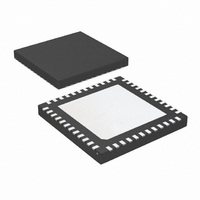
LMK03200ISQE/NOPB National Semiconductor, LMK03200ISQE/NOPB Datasheet - Page 20

LMK03200ISQE/NOPB
Manufacturer Part Number
LMK03200ISQE/NOPB
Description
IC CLOCK CONDITIONER PREC 48-LLP
Manufacturer
National Semiconductor
Type
Clock Conditionerr
Datasheet
1.LMK03200ISQENOPB.pdf
(40 pages)
Specifications of LMK03200ISQE/NOPB
Pll
Yes
Input
Clock
Output
LVDS, LVPECL
Number Of Circuits
1
Ratio - Input:output
1:9
Differential - Input:output
Yes/Yes
Frequency - Max
1.296GHz
Divider/multiplier
Yes/No
Voltage - Supply
3.15 V ~ 3.45 V
Operating Temperature
-40°C ~ 85°C
Mounting Type
Surface Mount
Package / Case
48-LLP
Frequency-max
1.296GHz
Lead Free Status / RoHS Status
Lead free / RoHS Compliant
Other names
LMK03200ISQETR
Available stocks
Company
Part Number
Manufacturer
Quantity
Price
Company:
Part Number:
LMK03200ISQE/NOPB
Manufacturer:
NSC
Quantity:
72
www.national.com
•
The device now begins the frequency calibration routine,
when it completes the LD pin will go high since PLL_MUX was
programmed with the active high option for the frequency cal-
ibration routine complete signal. When the LD pin goes high,
step 2 is executed.
Step 2
•
•
•
The device will now synchronize. As soon as the device is
settled the LD pin will go high to indicate the device is phase
locked (0_DELAY_MODE = 1 reverts the LD pin back to dig-
ital lock detect). Now the device's VCO will be locked to
1228.8 MHz with the output clocks of 12.288, 30.72, and
61.44 MHz.
2.3 Recommended Programming Sequence, bypassing
VCO divider
The programming procedure when using the VCO mux to by-
pass the VCO divider has two steps. The first step runs the
frequency calibration routine with the VCO divider in the feed-
back path. The second step bypasses the VCO divider and
locks the PLL.
Step 1
•
•
•
•
•
•
•
•
Now the LD pin should be monitored for the frequency cali-
bration routine completed signal to be asserted if PLL_MUX
was set to 3 or 4 and DLD_MODE2 = 1. Otherwise wait 2 ms
for the frequency calibration routine to complete. Once the
Begin monitoring LD pin for frequency calibration routine
complete signal.
GOE pin is set high.
Program Register 0
RESET = 0
0_DELAY_MODE = 1 (activate 0-delay mode)
DLD_MODE2 = 1 (same, don't care)
FB_MUX = 2 (CLKout6 feedback)
Program Register 15 (VCO Frequency = 1228.8 MHz)
PLL_N = 1 (updated value)
VCO_DIV = 2 (don't care)
PLL_CP_GAIN = Loop filter dependant
Program R0 with the reset bit set (RESET = 1). This
ensures the device is in a default state. When the reset bit
is set in R0, the other R0 bits are ignored.
— If R0 is programmed again, the reset bit is programmed
Program R0 to R7 as necessary with desired clocks with
appropriate enable, mux, divider, and delay settings.
— The outputs should be programmed with divider values
— R0: DLD_MODE2 = 1 (Digital Lock Detect is now
— R7: VCO_MUX = 0 (VCO divider output, default)
Program R8 for optimum phase noise performance.
Program R9 with Vboost setting if necessary.
Program R11 with DIV4 setting if necessary.
Program R13 with oscillator input frequency and internal
loop filter values.
Program R14 with Fout enable bit, global clock output bit,
power down setting, PLL mux setting, and PLL_R divider.
— R14: PLL_MUX = 3 or 4 for frequency calibration
Program R15 with PLL charge pump gain, VCO divider,
and PLL N divider. The frequency calibration routine
starts.
clear (RESET = 0).
which achieve desired output frequencies after the
VCO divider has been bypassed.
Frequency Calibration Routine Complete)
routine complete signal.
20
frequency calibration routine is completed step 2 may be ex-
ecuted to bypass the VCO divider.
Step 2
•
•
•
•
•
After a short settling time, the VCO will be locked and the
clock outputs will be at the desired frequency. The LD pin will
indicate when the PLL is locked if PLL_MUX is programmed
to a digital lock detect mode.
2.3.1 VCO divider bypass example
In this example assume the user requirements are: an input
reference of 61.44 MHz and clock output frequencies of 614.4
MHz on CLKout0 and CLKout1, and 307.2 MHz on CLKout2.
The VCO is programmed to 1228.8 MHz.
Registers not explicitly programmed are set to default values.
Step 1
•
•
•
•
•
•
•
•
Program R0 with the same settings as step 1 except:
— DLD_MODE2 = 0 (Digital lock detect is normal)
— 0_DELAY_MODE = 1 (temporarily enable 0-delay
Program R7
— VCO_MUX = 2 (VCO output)
Program R14 with PLL_MUX as desired, or PLL_MUX =
3 or 4 for Lock Detect.
Program R15 with the updated PLL_N value since the
VCO divider is no longer in the feedback path. The
updated value of PLL_N = Old PLL_N * VCO_Divider
value. This programs the VCO to the same frequency as
step 1. The VCO must be programmed for the same
frequency as step 1.
Program R0 with the same settings except:
— 0_DELAY_MODE = 0 (disable 0-delay mode)
GOE pin is set high
Program Register 0 (reset device)
RESET = 1
Other values don't matter
Program Register 0 again (614.4 MHz)
DLD_MODE2 = 1 (Digital Lock detect will be used for
monitoring frequency calibration routine complete)
CLKout0_EN = 1 (turn output on)
CLKout0_MUX = 0 (bypassed)
Program Register 1 (614.4 MHz)
CLKout1_EN = 1 (turn output on)
CLKout1_MUX = 0 (bypassed)
Program Register 2 (307.2 MHz)
CLKout2_EN = 2 (turn output on)
CLKout2_MUX = 1 (divide)
CLKout2_DIV = 1 (divide by 2)
Program Register 8
Program Register 14
PLL_R = 2 (Phase detector frequency = 30.72 MHz)
PLL_MUX = 3 (DLD Active High, now frequency
calibration routine complete)
Program Register 15 (VCO Frequency = 1228.8 MHz)
PLL_N = 20
VCO_DIV = 2
PLL_CP_GAIN = Loop filter dependant
Begin monitoring LD pin lock detect.
mode)
0_DELAY_MODE is not to be used in VCO divider
bypass mode. It is only activated briefly to prevent the
frequency calibration routine from running when R15 is
programmed while the VCO Mux is selecting the VCO
Output directly.


