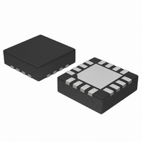
NB6N239SMNG ON Semiconductor, NB6N239SMNG Datasheet

NB6N239SMNG
Specifications of NB6N239SMNG
NB6N239SMNGOS
Available stocks
Related parts for NB6N239SMNG
NB6N239SMNG Summary of contents
Page 1
NB6N239S 3.3 V, 3.0 GHz Any Differential Clock IN to LVDS OUT ÷1/2/4/8, ÷2/4/8/16 Clock Divider Description The NB6N239S is a high−speed, low skew clock divider with two divider circuits, each having selectable clock divide ratios; B1/2/4/8 and B2/4/8/16. Both ...
Page 2
V Table 1. PIN DESCRIPTION Pin Name I CLK LVDS, LVPECL, CML, HSTL Input 3 CLK LVDS, LVPECL, CML, HSTL Input 4 V BBAC 5 EN* LVCMOS/LVTTL Input 6 SELB0* LVCMOS/LVTTL Input 7 SELB1* LVCMOS/LVTTL Input 8 ...
Page 3
SELA0 SELA1 CLK CLK EN SELB0 SELB1 + MR V BBAC Table 2. FUNCTION TABLE CLK EN Table 3. CLOCK DIVIDE SELECT, QA OUTPUTS SELA1* SELA0 ...
Page 4
Table 5. ATTRIBUTES Internal Input Pulldown Resistor Internal Input Pullup Resistor ESD Protection Moisture Sensitivity, Indefinite Time Out of Drypack (Note 1) Flammability Rating Transistor Count Meets or exceeds JEDEC Spec EIA/JESD78 IC Latchup Test 1. For additional Moisture Sensitivity ...
Page 5
Table 7. DC CHARACTERISTICS, CLOCK INPUTS, LVDS OUTPUTS ( 3.465 V, GND = Min Symbol Characteristic I Power Supply CC Current (Inputs and Outputs OPEN) V Output HIGH OH Voltage (Notes 2) V ...
Page 6
Table 8. DC CHARACTERISTICS, LVTTL/LVCMOS INPUTS Symbol Characteristic V Input HIGH Voltage (LVCMOS/LVTTL Input LOW Voltage (LVCMOS/LVTTL Input HIGH Current IH I Input LOW Current IL NOTE: Device will meet the specifications after thermal equilibrium has ...
Page 7
The NB6N239S is a high−speed, low skew clock divider with two divider circuits, each having selectable clock divide ratios; B1/2/4/8 and B2/4/8/16. Both divider circuits drive differential LVDS compatible outputs. The internal dividers are synchronous to each other. Therefore, the ...
Page 8
CLK Q (÷n) EN Figure 6. Output Enable Timing Diagrams The EN signal will “freeze” the internal divider flip−flops on the first falling edge of CLK after its assertion. The internal divider flip−flops will maintain their state during the freeze. ...
Page 9
NB6N239S CLK − 2 LVPECL Driver CLK GND Figure 12. LVPECL Interface ...
Page 10
CLOCK OUTPUT FREQUENCY (GHz) out Figure 18. Output Voltage Amplitude (V For 16; f CLK CLK PLH Figure 19. AC Reference Measurement NB6N239S Q ...
Page 11
... ORDERING INFORMATION Device NB6N239SMN NB6N239SMNG NB6N239SMNR2 NB6N239SMNR2G †For information on tape and reel specifications, including part orientation and tape sizes, please refer to our Tape and Reel Packaging Specifications Brochure, BRD8011/D. Resource Reference of Application Notes AN1405/D AN1406/D AN1503/D AN1504/D AN1568/D AN1672/D AND8001/D − Odd Number Counters Design AND8002/D − ...
Page 12
... Pb−Free strategy and soldering details, please download the ON Semiconductor Soldering and Mounting Techniques Reference Manual, SOLDERRM/D. N. American Technical Support: 800−282−9855 Toll Free USA/Canada Europe, Middle East and Africa Technical Support: Phone: 421 33 790 2910 Japan Customer Focus Center Phone: 81− ...


