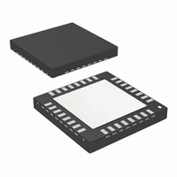
LMX2531LQ1700E/NOPB National Semiconductor, LMX2531LQ1700E/NOPB Datasheet - Page 20

LMX2531LQ1700E/NOPB
Manufacturer Part Number
LMX2531LQ1700E/NOPB
Description
IC PLL FREQ SYNTH W/VCO 36-LLP
Manufacturer
National Semiconductor
Series
PowerWise®r
Type
Clock/Frequency Synthesizer (RF)r
Datasheet
1.LMX2531LQ1778ENOPB.pdf
(36 pages)
Specifications of LMX2531LQ1700E/NOPB
Pll
Yes
Input
Clock
Output
CMOS
Number Of Circuits
1
Ratio - Input:output
2:2
Differential - Input:output
No/No
Frequency - Max
1.77GHz
Divider/multiplier
Yes/No
Voltage - Supply
2.8 V ~ 3.2 V
Operating Temperature
-40°C ~ 85°C
Mounting Type
Surface Mount
Package / Case
36-LLP
Frequency-max
1.77GHz
Number Of Elements
1
Supply Current
46mA
Pll Input Freq (min)
5MHz
Pll Input Freq (max)
80MHz
Operating Supply Voltage (typ)
3V
Operating Temp Range
-40C to 85C
Package Type
LLP EP
Output Frequency Range
1662 to 1770MHz
Operating Supply Voltage (min)
2.8V
Operating Supply Voltage (max)
3.2V
Operating Temperature Classification
Industrial
Pin Count
36
Leaded Process Compatible
Yes
Rohs Compliant
Yes
Peak Reflow Compatible (260 C)
Yes
Lead Free Status / RoHS Status
Lead free / RoHS Compliant
Other names
LMX2531LQ1700ETR
www.national.com
2.0 General Programming Information
The LMX2531 is programmed using 11 24-bit registers used to control the LMX2531 operation. A 24-bit shift register is used as a
temporary register to indirectly program the on-chip registers. The shift register consists of a data field and an address field. The
last 4 register bits, CTRL[3:0] form the address field, which is used to decode the internal register address. The remaining 20 bits
form the data field DATA[19:0]. While LE is low, serial data is clocked into the shift register upon the rising edge of clock (data is
programmed MSB first). When LE goes high, data is transferred from the data field into the selected register bank. Although there
are actually 14 registers in this part, only a portion of them should be programmed, since the state of the other hidden registers
(R13, R11, and R10) are set during the initialization sequence. Although it is possible to program these hidden registers, as well
as a lot of bits that are defined to either '1' or '0', the user should not experiment with these hidden registers and bits, since the
parts are not tested under these conditions and doing so will most likely degrade performance.
2.01 REGISTER LOCATION TRUTH TABLE
2.02 INITIALIZATION SEQUENCE
The initial loading sequence from a cold start is described below. The registers must be programmed in order shown. There must
be a minimum of 10 ms between the time when R5 is last loaded and R1 is loaded to ensure time for the LDOs to power up properly.
MSB
D19 D18 D17 D16 D15 D14 D13 D12 D11 D10 D9 D8 D7 D6 D5 D4 D3 D2 D1 D0 C3 C2 C1
REG.
INIT1
INIT2
R12
R5
R5
R5
R9
R8
R7
R6
R4
R3
R2
R1
R0
C3
1
1
1
0
0
0
0
0
0
0
0
23 22 21 20 19 18 17 16 15 14 13 12 11 10
1
1
1
0
0
0
0
0
0
Programming of this register is necessary under specific circumstances.
0
0
0
See individual section for Register R8 programming information.
See individual section for Register R7 programming information.
See individual section for Register R6 programming information.
See individual section for Register R4 programming information.
See individual section for Register R3 programming information.
See individual section for Register R2 programming information.
See individual section for Register R1 programming information.
See individual section for Register R0 programming information.
Register R4 only needs to be programmed if FastLock is used.
0
0
0
Program R12 as shown in the complete register map.
Program R9 as shown in the complete register map.
C2
1
0
0
1
1
1
1
0
0
0
0
1
0
0
0
0
0
0
0
0
DATA[19:0]
0
0
0
DATA[19:0]
0
0
0
0
0
0
C1
20
0
0
0
1
1
0
0
1
1
0
0
0
0
0
0
0
0
0
0
1
9
0
0
1
8
0
0
1
C0
0
1
0
1
0
1
0
1
0
1
0
7
0
0
1
6
0
0
1
5
0
0
1
4
0
0
1
Data Address
C3 C2 C1 C0
CONTROL[3:0]
3
0
0
0
1
1
1
0
0
0
0
0
0
0
R12
R9
R8
R7
R6
R5
R4
R3
R2
R1
R0
2
1
1
1
1
0
0
1
1
1
0
0
0
0
1
0
0
0
0
0
0
1
1
0
1
1
0
0
LSB
C0
0
1
1
1
0
1
0
1
0
0
1
0
1
0


