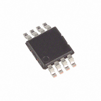
DS1099U-WA+T Maxim Integrated Products, DS1099U-WA+T Datasheet - Page 5

DS1099U-WA+T
Manufacturer Part Number
DS1099U-WA+T
Description
IC OSCILLATOR DUAL LOW-FRQ 8USOP
Manufacturer
Maxim Integrated Products
Series
EconOscillator™r
Type
Clock Generatorr
Datasheet
1.DS1099U-FF.pdf
(6 pages)
Specifications of DS1099U-WA+T
Pll
No
Input
Clock
Output
CMOS, TTL
Number Of Circuits
1
Ratio - Input:output
1:2
Differential - Input:output
No/No
Frequency - Max
2Hz, 1.048MHz
Divider/multiplier
Yes/No
Voltage - Supply
2.7 V ~ 5.5 V
Operating Temperature
-40°C ~ 125°C
Mounting Type
Surface Mount
Package / Case
8-MSOP, Micro8™, 8-uMAX, 8-uSOP,
Frequency-max
2Hz/1.048MHz
Lead Free Status / RoHS Status
Lead free / RoHS Compliant
Table 1. Divider Settings and Output
Frequencies
The DS1099 consists of a fixed-frequency 1.048MHz
master oscillator followed by two independent factory-
programmable dividers. The two divider outputs are
connected to pins OUT0 and OUT1, which are inde-
DIVIDER SETTING
X
0
OR X
19
20
21
22
—
0
1
2
3
4
5
1
_______________________________________________________________________________________
Detailed Description
GND
V
OE0
OE1
1,048,576
2,097,152
4,194,304
CC
DIVISOR
524,288
16
32
—
1
2
4
8
Low-Frequency Dual EconOscillator
PROGRAMMED
V
CC
FACTORY-
EEPROM
OSCILLATOR
f
OUT0
1.048MHz
MASTER
1.048MHz
0.524MHz
0.262MHz
0.131MHz
65.50kHz
32.75kHz
0.25Hz
f
0.5Hz
MOSC
2Hz
1Hz
OR f
—
OUT1
(X = X
(X = X
DIVIDE BY 2
DIVIDE BY 2
DIVIDER 0
DIVIDER 1
0
1
= 0...22)
= 0...22)
X
X
pendently enabled/disabled using the output-enable
pins, OE0 and OE1, respectively. When the output-
enable pins are active (low), the corresponding outputs
are enabled. If either output-enable pin is tied to its
inactive state (high), then the corresponding output is
disabled and forced high immediately. The output-
enable pins only disable the corresponding output
driver(s) and do not shut down the master oscillator or
the dividers.
Since the master oscillator frequency, f
the frequency of OUT0 and OUT1 is determined by
DIVIDER 0 and DIVIDER 1, respectively. And since
each output has its own divider, f
be programmed independent of each other.
The frequency of the outputs are calculated as follows:
where X
DIVIDER 1 setting. Valid values for X
gers 0 to 22 (dec).
Table 1 shows output frequencies and divider values
for the range of divider settings.
DS1099
f
f
OUT0
OUT1
0
is the DIVIDER 0 setting and X
= f
= f
OUTPUT
OUTPUT
DRIVER
DRIVER
MOSC
MOSC
f
f
/ 2
/ 2
Functional Diagram
OUT0
OUT1
X 0
X 1
OUT0
OUT1
= 1.048MHz / 2
= 1.048MHz / 2
OUT0
0
and X
MOSC
and f
X 0
X 1
1
OUT1
, is fixed,
1
are inte-
is the
can
5


