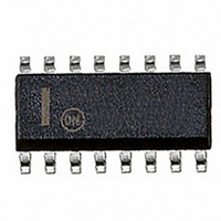
NB2308AI2DR2G ON Semiconductor, NB2308AI2DR2G Datasheet - Page 6

NB2308AI2DR2G
Manufacturer Part Number
NB2308AI2DR2G
Description
IC BUFFER CLK 8OUT 3.3V 16-SOIC
Manufacturer
ON Semiconductor
Type
Zero Delay Bufferr
Datasheet
1.NB2308AI1DR2G.pdf
(12 pages)
Specifications of NB2308AI2DR2G
Pll
Yes with Bypass
Input
Clock
Output
Clock
Number Of Circuits
1
Ratio - Input:output
1:8
Differential - Input:output
No/No
Frequency - Max
133.3MHz
Divider/multiplier
Yes/Yes
Voltage - Supply
3 V ~ 3.6 V
Operating Temperature
-40°C ~ 85°C
Mounting Type
Surface Mount
Package / Case
16-SOIC (3.9mm Width)
Frequency-max
133MHz
Lead Free Status / RoHS Status
Lead free / RoHS Compliant
Available stocks
Company
Part Number
Manufacturer
Quantity
Price
Company:
Part Number:
NB2308AI2DR2G
Manufacturer:
ON Semiconductor
Quantity:
1 900
Zero Delay and Skew Control
Delay between input and output.
OUTPUT
OUTPUT
All outputs should be uniformly loaded to achieve Zero
--1000
--1500
1500
1000
--500
500
OUTPUT LOAD DIFFERENCE: FBK LOAD -- CLKA/CLKB LOAD (pF)
Figure 3. REF Input to CLKA/CLKB Delay vs.
--30 --25 --20 --15 --10
Difference in Loading between FBK Pin and
0
Figure 6. Output - - Output Skew
1.4 V
t
Figure 4. Duty Cycle Timing
5
1.4 V
CLKA/CLKB Pins
t
2
1.4 V
FBK_Device 1
FBK_Device 2
1.4 V
--5
t
1
0
5
1.4 V
10
t
7
15
V
Figure 8. Device - - Device Skew
2
SWITCHING WAVEFORMS
DD
20
http://onsemi.com
25
V
2
DD
30
OUTPUT
6
can be driven from any of the eight available output pins.
The output driving the FBK pin will be driving a total load
of 7 pF plus any additional load that it drives. The relative
loading of this output (with respect to the remaining outputs)
can adjust the input- -output delay. This is shown in Figure 3.
outputs including the one providing feedback should be
equally loaded. If input- -output delay adjustments are
required, use the above graph to calculate loading
differences between the feedback output and remaining
outputs. For zero output- -output skew, be sure to load
outputs equally.
To close the feedback loop of the NB2308A, the FBK pin
For applications requiring zero input- -output delay, all
OUTPUT
INPUT
Figure 5. All Outputs Rise/Fall Time
t
0.8 V
3
2.0 V
Figure 7. Input - - Output Propagation Delay
t
6
V
2
DD
V
2.0 V
2
DD
0.8 V
t
4
0 V
3.3 V


