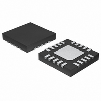
MAX9491ETP095+ Maxim Integrated Products, MAX9491ETP095+ Datasheet - Page 6

MAX9491ETP095+
Manufacturer Part Number
MAX9491ETP095+
Description
IC FACT-PROG PLL CLK GEN 20-TQFN
Manufacturer
Maxim Integrated Products
Type
PLL Clock Generatorr
Datasheet
1.MAX9491ETP010T.pdf
(11 pages)
Specifications of MAX9491ETP095+
Pll
Yes
Input
LVCMOS, Crystal
Output
LVCMOS
Number Of Circuits
1
Ratio - Input:output
1:1
Differential - Input:output
No/No
Frequency - Max
200MHz
Divider/multiplier
No/No
Voltage - Supply
3 V ~ 3.6 V
Operating Temperature
-40°C ~ 85°C
Mounting Type
Surface Mount
Package / Case
20-TQFN Exposed Pad
Frequency-max
200MHz
Lead Free Status / RoHS Status
Lead free / RoHS Compliant
The MAX9491 features a programmable fractional-N
PLL, so frequencies between 4MHz to 200MHz can be
generated. The device provides a buffered PLL clock
output. The crystal input frequency can be between
5MHz and 35MHz, and the clock input between 5MHz
and 50MHz. The internal VCXO has a fine-tuning range
of ±200ppm.
Driving PD low places the MAX9491 in power-down
mode. PD then sets CLK_OUT to high impedance and
Factory Programmable Single PLL
Clock Generator
6
6–9, 14, 19, 20
12, 13, 16
_______________________________________________________________________________________
4, 10, 11
TQFN
EP
15
17
18
1
2
3
5
PIN
2, 3, 8, 10
TSSOP
6, 9, 11
4, 12
OR REFERENCE
INPUT
13
14
—
—
—
5
7
1
Detailed Description
CLK_OUT
NAME
AGND
TUNE
V
GND
V
I.C.
DDA
PD
X2
X1
EP
DD
Power-Down
0.1µF
VCXO Tune Voltage Input. If using a reference clock input or VCXO is not used,
connect TUNE to V
Analog Power Supply. Bypass to GND with a 0.1µF capacitor.
Analog Ground
Ground
Output Clock. Internally pulled down.
Internally Connected. Leave unconnected for normal operation.
Power Supply. Bypass to GND with a 0.1µF capacitor.
Active-Low Power-Down Input. Pull high for normal operation. Drive PD low to place
MAX9491 in power-down mode. Internally pulled down.
Crystal Connection 2. Leave unconnected if using a reference clock.
Crystal Connection 1 or Reference Clock Input
Exposed Paddle (TQFN Only). Connect EP to GND or leave unconnected.
TUNE
C1
C2
+3.3V
V
X1
X2
AGND
GND
Typical Operating Circuit/Block Diagram
DDA
VCXO
DD
shuts down the PLL. CLK_OUT has an 80kΩ (typ) inter-
nal pulldown resistor.
The MAX9491’s internal VCXO produces a reference
clock for the PLL used to generate the CLK_OUT. The
oscillator uses a crystal as the base frequency refer-
ence and has a voltage-controlled tuning input for micro
adjustment in a ±200ppm range. The tuning voltage,
V
crystal should be AT-cut and oscillate on its fundamen-
tal mode with ±30ppm. The crystal shunt capacitor
.
TUNE
MAX9491
PLL
OTP
, can vary from 0 to 3V as shown in Figure 1. The
Voltage-Controlled Crystal Oscillator
FUNCTION
CLK_OUT
V
V
V
PD
DD
DD
DD
+3.3V
0.1µF x 3
Pin Description
(VCXO)


