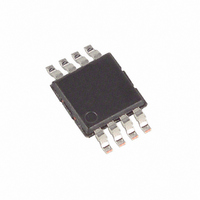
DS1094LU-42M+ Maxim Integrated Products, DS1094LU-42M+ Datasheet - Page 10

DS1094LU-42M+
Manufacturer Part Number
DS1094LU-42M+
Description
IC ECONOSCILLATOR SS 8-USOP
Manufacturer
Maxim Integrated Products
Series
EconOscillator™r
Type
Clock Generatorr
Datasheet
1.DS1094LU-42M.pdf
(11 pages)
Specifications of DS1094LU-42M+
Pll
No
Input
Clock
Output
Clock
Number Of Circuits
1
Ratio - Input:output
2:4
Differential - Input:output
No/No
Frequency - Max
2MHz
Divider/multiplier
Yes/No
Voltage - Supply
3 V ~ 3.6 V
Operating Temperature
-40°C ~ 85°C
Mounting Type
Surface Mount
Package / Case
8-MSOP, Micro8™, 8-uMAX, 8-uSOP,
Frequency-max
2MHz
Lead Free Status / RoHS Status
Lead free / RoHS Compliant
that are transferred (most significant bit first) from the
slave to the master are read by the master using the bit
read definition above, and the master transmits an ACK
using the bit write definition to receive additional data
bytes. The master must NACK the last byte read to ter-
minate communication so the slave will return control of
SDA to the master.
Slave Address Byte: The slave address byte consists of
a 7-bit slave address followed by the
4). The slave address is the most significant 7 bits and
the R/W bit is the least significant bit. The 3 address bits
in the slave address (A2 to A0) permit a maximum of
eight DS1094Ls to share the same 2-wire bus.
Each slave on the 2-wire bus has a unique slave
address, which is used by the master to select which
slave it wishes to communicate with. Following a start
condition, all slaves on the 2-wire bus await the slave
address byte from the master. Each slave compares its
own slave address with the slave address sent from the
master. If the slave address matches, the slave
acknowledges and continues communication with the
master (based on the R/W bit). Otherwise, if the slave
address does not match, the slave ignores communica-
tion until the next start condition.
When the R/W bit is zero, the master writes data to the
specified slave. When the R/W is one, the master reads
data from the specified slave.
Memory Address: During a 2-wire write operation, the
master must transmit a memory address to identify the
memory location where the slave is to store the data.
The memory address is always the second byte trans-
mitted during a write operation following the slave
address byte (R/W = 0).
Writing a Single Byte to a Slave: The master must
generate a start condition, write the slave address byte
(with R/W = 0), write the memory address, write the
byte of data, and generate a stop condition. The master
must read the slave’s acknowledgement following each
byte write.
Multiphase Spread-Spectrum EconOscillator
Figure 4. Slave Address Byte
10
____________________________________________________________________
*THESE BITS MUST MATCH THE
CORRESPONDING BITS IN THE ADDR REGISTER.
MSB
1
0
7-BIT SLAVE ADDRESS
1
1
2-Wire Communication
A2*
A1*
READ/WRITE BIT
A0*
R/W bit (see Figure
R/W
LSB
Acknowledge Polling: Any time EEPROM is written,
the EEPROM write time (t
stop condition to write to EEPROM. During the EEP-
ROM write time, the DS1094L will not acknowledge its
slave address because it is busy. It is possible to take
advantage of this phenomenon by repeatedly address-
ing the DS1094L until it finally acknowledges its slave
address. The alternative to acknowledge polling is to
wait for maximum period of t
attempting to write to EEPROM again.
Reading a Single Byte from a Slave: A dummy write
cycle is used to read a particular register. To do this
the master generates a start condition, writes the slave
address byte (with R/W = 0), writes the memory
address of the desired register to read, generates a
repeated start condition, writes the slave address byte
(with R/W = 1), reads the register and follows with a
NACK (since only one byte is read), and generates a
stop condition. See Figure 5 for examples of reading
DS1094L registers.
SDA is an open-collector output and requires a pullup
resistor to realize high logic levels. Because the
DS1094L does not utilize clock cycle stretching, a mas-
ter using either an open-collector output with a pullup
resistor or CMOS output driver (push-pull) can be uti-
lized for SCL. Pullup resistor values should be chosen
to ensure that the rise and fall times listed in the AC
electrical characteristics are within specification.
If the DS1094L is used stand-alone (without a 2-wire
master), SDA and SCL should not be left unconnected,
or floating. It is recommended that pullup resistors be
used on both SDA and SCL to prevent the pins from
floating to unknown voltages and transitions. Likewise,
pullups are recommended over tying SDA and SCL
directly to V
To achieve best results, it is highly recommended that
a decoupling capacitor is used on the IC power supply
pins. Typical values of decoupling capacitors are
0.01µF and 0.1µF. Use high-quality, ceramic, surface-
mount capacitors. Mount the capacitors as close as
possible to the V
lead inductance.
CC
to allow future programmability.
CC
SDA and SCL Pullup Resistors
Application Information
and GND pins of the IC to minimize
Power-Supply Decoupling
Stand-Alone Operation
W
) is required following the
W
to elapse before


