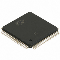
CY7B993V-2AC Cypress Semiconductor Corp, CY7B993V-2AC Datasheet

CY7B993V-2AC
Specifications of CY7B993V-2AC
Available stocks
Related parts for CY7B993V-2AC
CY7B993V-2AC Summary of contents
Page 1
... Cypress Semiconductor Corporation Document #: 38-07127 Rev. *E High-speed Multi-phase PLL Clock Buffer Functional Description The CY7B993V and CY7B994V High-speed Multi-phase PLL Clock Buffers offer user-selectable control over system clock functions. This multiple-output clock driver provides the system integrator with functions necessary to optimize the timing of high-performance computer and communication systems ...
Page 2
... GND 17 2DS1 18 1DS1 19 VCCQ 20 4DS0 21 3DS0 22 2DS0 23 1DS0 24 GND Document #: 38-07127 Rev. *E 100-pin TQFP CY7B993/ RoboClock CY7B994V CY7B993V VCCQ 74 REFA+ 73 REFA – 72 REFSEL 71 REFB– 70 REFB+ 69 2F0 GND 66 2QA0 65 VCCN 64 2QA1 63 GND 62 GND 61 2QB0 60 VCCN 59 2QB1 58 GND 57 FBF0 56 1F0 55 GND 54 VCCQ ...
Page 3
... Table 1). Feedback Output Phase Function Select: This input determines the phase function of the Feedback bank’s QFA[0:1] outputs (see Table 3). , LOW indicates a connection to GND, and MID indicates an open connection. Internal termination CC /2. RoboClock CY7B994V CY7B993V VCCQ FBKA– FBKA+ FBKB– ...
Page 4
... These two blocks, along with the VCO, form a PLL that tracks the incoming REF signal. The CY7B993V/994V have a flexible REF and FB input scheme. These inputs allow the use of either differential LVPECL or single-ended LVTTL inputs. To configure as single-ended LVTTL inputs, the complementary pin must be left open (internally pulled to 1 ...
Page 5
... REF. For example, if the output used for feedback is programmed to shift –8t forward in time skew will effectively be skewed 16t ) of the V NOM CO when the output connected undivided. NOM RoboClock CY7B994V CY7B993V Output Skew Function Bank1 Bank2 Bank3 Bank4 –4t –4t –8t –8t U ...
Page 6
... When a bank of outputs is disabled to HI-Z state, the respective bank of outputs will go HI-Z immediately. Table 5. DIS[1:4]/FBDIS Pin Functionality OUTPUT_MODE DIS[1:4]/FBDIS HIGH/LOW LOW HIGH HIGH LOW HIGH MID X RoboClock CY7B994V CY7B993V Output Mode ENABLED HI-Z HOLD-OFF FACTORY TEST Page ...
Page 7
... MHz is 16 (with 25-pF load and 0-m/s air flow). Typical Safe Operating Zone (25-pF Load, 0-m /s air flow ) Safe Operating Zone Num ber of Outputs at 185 MHz Figure 2. Typical Safe Operating Zone RoboClock CY7B994V CY7B993V Page ...
Page 8
... –2 mA Min mA Min. < V Min. < GND Max Max Min. < V Min. < V Min. < GND IN RoboClock CY7B994V CY7B993V Ambient Temperature +70 C 3.3V – +85 C 3.3V Min. Max. = –30 mA 2.4 – Min. 2.4 – – 0 Min. – 0.5 CC –100 100 < Max ...
Page 9
... MHz for CY7B993V 200 MHz for NOM NOM at maximum frequency and maximum CCN Page Unit Unit pF Unit MHz MHz MHz MHz ...
Page 10
... OUTPUT C L < 185 MHz 200 MHz (a) LVTTL AC Test Load 3.3V 2.0V 0.8V GND < (b) TTL Input Test Waveform = 185 MHz 200 MHz. L RoboClock CY7B994V CY7B993V CY7B993/4V-2 CY7B993/4V-5 Min. Max. Min. Max. Unit – 500 – 700 ps – 200 – 200 ps 2 ...
Page 11
... Q REF TO DEVICE 1 and DEVICE1 t PDELTA FB DEVICE2 Q t SKEW2 INVERTED Q Ordering Information Propagation Max. Speed Delay (ps) (MHz) Ordering Code 250 100 CY7B993V-2AC 250 100 CY7B993V-2AI 250 200 CY7B994V-2AC 250 200 CY7B994V-2BBC 250 200 CY7B994V-2AI 250 200 CY7B994V-2BBI 500 100 CY7B993V-5AC 500 100 ...
Page 12
... Package Diagrams 100-pin Thin Plastic Quad Flat Pack (TQFP) A100 Document #: 38-07127 Rev. *E RoboClock CY7B994V CY7B993V 51-85048-*B Page ...
Page 13
... The inclusion of Cypress Semiconductor products in life-support systems application implies that the manufacturer assumes all risk of such use and in doing so indemnifies Cypress Semiconductor against all charges. RoboClock CY7B994V CY7B993V 51-85107-*B Page ...
Page 14
... Added three industrial packages HWT Added TTB Features RBI Power-up requirements to operating conditions information RGL Added min. F value of 12 MHz for CY7B993V and 24 MHz for CY7B994V out to switching characteristics table Corrected prop delay limit parameter from (t Output Description paragraph RGL Added clock input frequency (f ...


