LMX2352TMX/NOPB National Semiconductor, LMX2352TMX/NOPB Datasheet - Page 11
LMX2352TMX/NOPB
Manufacturer Part Number
LMX2352TMX/NOPB
Description
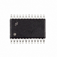
IC FREQ SYNTHESIZER DUAL 24TSSOP
Manufacturer
National Semiconductor
Series
PLLatinum™r
Type
PLL Frequency Synthesizerr
Datasheet
1.LMX2352TMNOPB.pdf
(21 pages)
Specifications of LMX2352TMX/NOPB
Pll
Yes with Bypass
Input
CMOS, TTL
Output
CMOS
Number Of Circuits
1
Ratio - Input:output
3:3
Differential - Input:output
Yes/No
Frequency - Max
1.2GHz, 550MHz
Divider/multiplier
Yes/No
Voltage - Supply
2.7 V ~ 5.5 V
Operating Temperature
-40°C ~ 85°C
Mounting Type
Surface Mount
Package / Case
24-TSSOP
Frequency-max
1.2GHz
Lead Free Status / RoHS Status
Lead free / RoHS Compliant
Other names
LMX2352TMX
LMX2352TMXTR
LMX2352TMXTR
Available stocks
Company
Part Number
Manufacturer
Quantity
Price
Company:

Part Number:
LMX2352TMX/NOPB
Manufacturer:
ST
Quantity:
7 600


Functional Description
and 3.2.2). The phase detector also receives a feedback
signal from the charge pump, in order to eliminate dead
zone.
1.5 Charge Pump
The phase detector’s current source outputs pump charge
into an external loop filter, which then converts the charge
into the VCO’s control voltage. The charge pumps steer the
charge pump output, CPo, to Vcc (pump-up) or ground
(pump-down). When locked, CPo is primarily in a
TRI-STATE
pump output current magnitude is programmable from 100
µA to 1.6 mA in 100 µA steps as shown in table in program-
ming description 3.2.2. The IF charge pump is set to either
100µA or 800µA levels using bit IF_R [19] (see programming
description 3.1.4).
1.6 Voltage Doubler
The Vp
supply over a range of Vcc to 5.5v to provide current for the
RF charge pump circuit. An internal voltage doubler circuit
connected between the Vcc and VpRF supply pins alter-
nately allows Vcc = 3v (
pump circuit at close to twice the Vcc power supply voltage.
The voltage doubler mode is enabled by setting the V2_EN
bit (RF_R [22]) to a HIGH level. The voltage doubler’s
charge pump driver originates from the RF oscillator input
(OSCx). The device will not totally powerdown until the
V2_EN bit is programmed low. The average delivery current
of the doubler is less than the instantaneous current demand
of the RF charge pump when active and is thus not capable
of sustaining a continuous out of lock condition. A large
external capacitor connected to Vp
control power supply droop when changing frequencies. Re-
fer to the application note AN-1119 for more details.
1.7 MICROWIRE
The programmable functions are accessed through the MI-
CROWIRE serial interface. The interface is made of 3 func-
tions: clock, data and latch enable (LE). Serial data for the
various counters is clocked in from data on the rising edge of
clock, into the 24- bit shift register. Data is entered MSB first.
The last two bits decode the internal register address. On the
rising edge of LE, data stored in the shift register is loaded
into one of the 4 appropriate latches (selected by address
bits). A complete programming description is included in the
following sections.
1.8 Fo/LD Multifunction Output
The Fo/LD output pin can deliver several internal functions
including analog/digital lock detects, and counter outputs.
See programming description 3.1.5 for more details.
1.8.1 Lock Detect
A digital filtered lock detect function is included with each
phase detector through an internal digital filter to produce a
logic level output available on the Fo/LD output pin if se-
lected. The lock detect output is high when the error between
the phase detector inputs is less than 15 nsec for 5 consecu-
tive comparison cycles. The lock detect output is low when
the error between the phase detector outputs is more than
30 nsec for one comparison cycle. An analog lock detect
RF
pin is normally driven from an external power
®
mode with small corrections. The RF charge
™
Serial Interface
±
10%) users to run the RF charge
RF
is therefore needed to
(Continued)
11
signal is also selectable. The lock detect output is always low
when the PLL is in power down mode. See programming
descriptions 3.1.5, 4.6 - 4.8 for more details.
1.9 Power Control
Each PLL is individually power controlled by device enable
pins or MICROWIRE power down bits. The enable pins
override the power down bits except for the V2_EN bit. The
RF_EN pin controls the RF PLL; IF_EN pin controls the IF
PLL. When both pins are high, the power down bits deter-
mine the state of power control (see programming descrip-
tion 3.2.1.2). Activation of any PLL power down mode results
in the disabling of the respective N counter and de-biasing of
its respective Fin input (to a high impedance state). The R
counter functionality also becomes disabled when the power
down bit is activated. The reference oscillator block powers
down and the OSCin pin reverts to a high impedance state
when both RF and IF enable pins or power down bit’s are
asserted, unless the V2_EN bit (RF_R[22]) is high. Power
down forces the respective charge pump and phase com-
parator logic to a TRI-STATE condition. A power down
counter reset function resets both N and R counters. Upon
powering up the N counter resumes counting in “close”
alignment with the R counter (The maximum error is one
prescaler cycle). The MICROWIRE control register remains
active and capable of loading and latching in data during all
of the power down modes.
www.national.com
Related parts for LMX2352TMX/NOPB
Image
Part Number
Description
Manufacturer
Datasheet
Request
R

Part Number:
Description:
07B5847
Manufacturer:
National Semiconductor
Datasheet:

Part Number:
Description:
IC FREQ SYNTHESIZER DUAL 24TSSOP
Manufacturer:
National Semiconductor
Datasheet:

Part Number:
Description:
National Semiconductor [8-Bit D/A Converter]
Manufacturer:
National Semiconductor
Datasheet:
Part Number:
Description:
National Semiconductor [Media Coprocessor]
Manufacturer:
National Semiconductor
Datasheet:
Part Number:
Description:
Digitally Controlled Tone and Volume Circuit with Stereo Audio Power Amplifier, Microphone Preamp Stage and National 3D Sound
Manufacturer:
National Semiconductor
Datasheet:
Part Number:
Description:
Digitally Controlled Tone and Volume Circuit with Stereo Audio Power Amplifier, Microphone Preamp Stage and National 3D Sound
Manufacturer:
National Semiconductor
Datasheet:
Part Number:
Description:
AC97 Rev 2 Codec with Sample Rate Conversion and National 3D Sound
Manufacturer:
National Semiconductor
Part Number:
Description:
Manufacturer:
National Semiconductor
Datasheet:
Part Number:
Description:
Manufacturer:
National Semiconductor
Datasheet:
Part Number:
Description:
General Purpose, Low Voltage, Low Power, Rail-to-Rail Output Operational Amplifiers
Manufacturer:
National Semiconductor
Datasheet:
Part Number:
Description:
8-bit 20 MSPS flash A/D converter.
Manufacturer:
National Semiconductor
Datasheet:
Part Number:
Description:
Low Noise Quad Operational Amplifier
Manufacturer:
National Semiconductor
Datasheet:
Part Number:
Description:
Quad Differential Line Receivers
Manufacturer:
National Semiconductor
Datasheet:
Part Number:
Description:
Quad High Speed Trapezoidal? Bus Transceiver
Manufacturer:
National Semiconductor
Datasheet: