MPC9239FN Freescale Semiconductor, MPC9239FN Datasheet
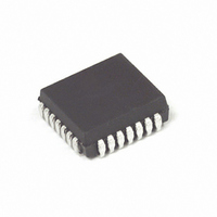
IC PECL CLOCK LV 900MHZ 28-PLCC

MPC9239FN

Manufacturer Part Number
MPC9239FN
Description
IC PECL CLOCK LV 900MHZ 28-PLCC
Manufacturer
Freescale Semiconductor
Type
Clock/Frequency Synthesizer, Clock Generator, Multiplexerr
Datasheet

Specifications of MPC9239FN

Pll
Yes with Bypass
Input
LVCMOS
Output
LVCMOS, LVPECL
Number Of Circuits
1
Ratio - Input:output
1:1
Differential - Input:output
No/Yes
Frequency - Max
900MHz
Divider/multiplier
Yes/Yes
Voltage - Supply
3.135 V ~ 3.465 V
Operating Temperature
0°C ~ 70°C
Mounting Type
Surface Mount
Package / Case
28-PLCC
Frequency-max
900MHz
Lead Free Status / RoHS Status
Contains lead / RoHS non-compliant

Available stocks

Company
Part Number
Manufacturer
Quantity
Price
Part Number:
MPC9239FN
Manufacturer:
Freescale Semiconductor
Quantity:
10 000
Part Number:
MPC9239FNR2
Manufacturer:
MOTOROLA/摩托罗拉
Quantity:
20 000
Freescale Semiconductor
Technical Data
© Freescale Semiconductor, Inc., 2005. All rights reserved.
900 MHz Low Voltage LVPECL
Clock Synthesizer
high performance clock generation in mid-range to high-performance telecom,
networking, and computing applications. With output frequencies from
3.125 MHz to 900 MHz and the support of differential LVPECL output signals the
device meets the needs of the most demanding clock applications.
Features
Functional Description
its frequency reference. The frequency of the internal crystal oscillator or external
reference clock signal is multiplied by the PLL. The VCO within the PLL operates over a range of 800 to 1800 MHz. Its output is
scaled by a divider that is configured by either the serial or parallel interfaces. The crystal oscillator frequency f
feedback-divider M and the PLL post-divider N determine the output frequency.
by adjusting the VCO control voltage. Note that for some values of M (either too high or too low) the PLL will not achieve phase
lock. The PLL will be stable if the VCO frequency is within the specified VCO frequency range (800 to 1800 MHz). The M-value
must be programmed by the serial or parallel interface.
ratios (1, 2, 4, or 8). This divider extends performance of the part while providing a 50% duty cycle. The output driver is driven
differentially from the output divider, and is capable of driving a pair of transmission lines terminated 50 Ω to V
positive supply voltage for the internal PLL is separated from the power supply for the core logic and output drivers to minimize
noise induced jitter.
inputs to configure the internal counters. It is recommended on system reset to hold the P_LOAD input LOW until power becomes
valid. On the LOW-to-HIGH transition of P_LOAD, the parallel inputs are captured. The parallel interface has priority over the
serial interface. Internal pullup resistors are provided on the M[6:0] and N[1:0] inputs prevent the LVCMOS compatible control
inputs from floating. The serial interface centers on a twelve bit shift register. The shift register shifts once per rising edge of the
S_CLOCK input. The serial input S_DATA must meet setup and hold timing as specified in the AC Characteristics section of this
document. The configuration latches will capture the value of the shift register on the HIGH-to-LOW edge of the S_LOAD input.
Refer to the programming section for more information. The TEST output reflects various internal node values, and is controlled
by the T[2:0] bits in the serial data stream. In order to minimize the PLL jitter, it is recommended to avoid active signal on the
TEST output. The PWR_DOWN pin, when asserted, will synchronously divide the f
clocked by the PLL reference clock, thereby causing the frequency reduction to happen relatively slowly. Upon de-assertion of
the PWR_DOWN pin, the f
The MPC9239 is a 3.3 V compatible, PLL based clock synthesizer targeted for
The internal crystal oscillator uses the external quartz crystal as the basis of
The feedback path of the PLL is internal. The PLL adjusts the VCO output frequency to be M times the reference frequency
The PLL post-divider N is configured through either the serial or the parallel interfaces, and can provide one of four division
The configuration logic has two sections: serial and parallel. The parallel interface uses the values at the M[6:0] and N[1:0]
3.125 MHz to 900 MHz synthesized clock output signal
Differential LVPECL output
LVCMOS compatible control inputs
On-chip crystal oscillator for reference frequency generation
Alternative LVCMOS compatible reference input
3.3 V power supply
Fully integrated PLL
Minimal frequency overshoot
Serial 3-wire programming interface
Parallel programming interface for power-up
28 PLCC and 32 LQFP packaging
28-lead and 32-lead Pb-free package available
SiGe Technology
Ambient temperature range 0°C to + 70°C
Pin and function compatible to the MC12439
OUT
input will step back up to its programmed frequency in four discrete increments.
OUT
by 16. The power down sequence is
900 MHz LOW VOLTAGE
CLOCK SYNTHESIZER
MPC9239
28-LEAD PLCC PACKAGE
32-LEAD LQFP PACKAGE
Pb-FREE PACKAGE
Pb-FREE PACKAGE
CASE 873A-04
CASE 873A-04
CASE 776-02
CASE 776-02
AC SUFFIX
FN SUFFIX
FA SUFFIX
EI SUFFIX
Rev. 3, 08/2005
CC
XTAL
– 2.0 V. The
, the PLL
MPC9239

Related parts for MPC9239FN

MPC9239FN Summary of contents

Page 1

... PLL reference clock, thereby causing the frequency reduction to happen relatively slowly. Upon de-assertion of the PWR_DOWN pin, the f input will step back up to its programmed frequency in four discrete increments. OUT © Freescale Semiconductor, Inc., 2005. All rights reserved. MPC9239 Rev. 3, 08/2005 MPC9239 ...

Page 2

... SHIFT REGISTER Figure 1. MPC9239 Logic Diagram GND N[ TEST XTAL_SEL GND M[ OUT M[ OUT M[ Figure 3. MPC9239 32-Lead LQFP Pinout 11 1 ÷ TEST 3 T-LATCH BITS 0 MPC9239 (Top View) Advanced Clock Drivers Devices Freescale Semiconductor f OUT f OUT TEST NC M[3] M[2] M[1] M[0] P_LOAD OE XTAL_OUT ...

Page 3

... Advanced Clock Drivers Devices Freescale Semiconductor Type Analog Crystal oscillator interface. LVCMOS Alternative PLL reference input. LVPECL Differential clock output. LVCMOS Test and device diagnosis output. LVCMOS PLL reference select input. LVCMOS Configuration input for power down mode. Assertion (deassertion) of power down will decrease (increase) the output frequency by a ratio discrete steps ...

Page 4

... MIL-SPEC 883E 23.0 26.3 Method 1012.1 Min Max Unit –0.3 3.9 V –0 0 –0 0 ±20 mA ±50 mA °C –65 125 Advanced Clock Drivers Devices Freescale Semiconductor Condition ...

Page 5

... PLL feedback divider M must match the VCO frequency range: f XTAL 3. The frequency of S_CLOCK is limited to 10 MHz in serial programming mode. S_CLOCK can be switched at higher frequencies when used as test clock in test mode 6. Refer to the application section for more details. Advanced Clock Drivers Devices Freescale Semiconductor = 0°C to +70°C) A Min 2.0 V – ...

Page 6

... Advanced Clock Drivers Devices Freescale Semiconductor ...

Page 7

... M[6:0] and N[1:0] inputs into the M and N counters. When the P_LOAD signal Advanced Clock Drivers Devices Freescale Semiconductor is LOW the input latches will be transparent and any changes on the M[6:0] and N[1:0] inputs will affect the f ...

Page 8

... DC resistance inductor is required (less than 15 Ω). illustrates a typical V current (the CC_PLL Configuration S_CLOCK ÷ N (2) M-Counter out Last Bit = 10-15 Ω CC_PLL = 22 µ 0.01...0.1 µ Figure 5. V Power Supply Filter CC_PLL Advanced Clock Drivers Devices Freescale Semiconductor (1) CC_PLL MPC9239 ...

Page 9

... XTAL Figure 6. PCB Board Layout Recommendation for the PLCC28 Package Advanced Clock Drivers Devices Freescale Semiconductor Using the On-Board Crystal Oscillator The MPC9239 features a fully integrated on-board crystal oscillator to minimize system implementation costs. The oscillator is a series resonant, multivibrator type design as opposed to the more common parallel resonant oscillator design ...

Page 10

... MILLIMETERS MIN MAX 12.32 12.57 12.32 12.57 4.20 4.57 2.29 2.79 0.33 0.48 1.27 BSC 0.66 0.81 0.51 --- 0.64 --- 11.43 11.58 11.43 11.58 1.07 1.21 1.07 1.21 1.07 1.42 --- 0.50 2˚ 10˚ 10.42 10.92 1.02 --- Advanced Clock Drivers Devices Freescale Semiconductor ...

Page 11

... Advanced Clock Drivers Devices Freescale Semiconductor PACKAGE DIMENSIONS CASE 873A-04 ISSUE C 32-LEAD LQFP PACKAGE PAGE MPC9239 11 ...

Page 12

... MPC9239 12 PACKAGE DIMENSIONS CASE 873A-04 ISSUE C 32-LEAD LQFP PACKAGE PAGE Advanced Clock Drivers Devices Freescale Semiconductor ...

Page 13

... Advanced Clock Drivers Devices Freescale Semiconductor PACKAGE DIMENSIONS CASE 873A-04 ISSUE C 32-LEAD LQFP PACKAGE PAGE MPC9239 13 ...

Page 14

... Freescale Semiconductor product could create a situation where personal injury or death may occur. Should Buyer ...

Related keywords