LMX2313USLDX/NOPB National Semiconductor, LMX2313USLDX/NOPB Datasheet
LMX2313USLDX/NOPB
Specifications of LMX2313USLDX/NOPB
LMX2313USLDXTR
Available stocks


Related parts for LMX2313USLDX/NOPB

LMX2313USLDX/NOPB Summary of contents
Page 1
... The LMX2310/1/2/3U are manufactured using National’s 0.5µ ABiC V silicon BiCMOS process and is available in 20-pin CSP packages. Functional Block Diagram PLLatinum ™ trademark of National Semiconductor Corporation. © 2003 National Semiconductor Corporation LMX2311U 2.0 GHz LMX2313U 600 MHz Features n RF operation up to 2.5 GHz n 2 ...
Page 2
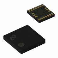
Connection Diagram www.national.com 20-Pin Thin Chip Scale Package NS Package Number SLD20A 2 20043823 ...
Page 3
Pin Descriptions Pin Number Pin Name I — No Connect Charge Pump output. For connection GND — Analog ground INB 6 OSC — ...
Page 4
Pin Descriptions (Continued) Pin Number Pin Name Data GND µ www.national.com I/O Description — No Connect. I High impedance CMOS ...
Page 5
... Absolute Maximum Ratings 2) If Military/Aerospace specified devices are required, please contact the National Semiconductor Sales Office/ Distributors for availability and specifications. Power Supply Voltage µC Voltage on any pin with GND= FL OSC , OSC ( OUT i Data, Clock, LE, CE, FoLD ( Storage Temperature Range Electrical Characteristics < ...
Page 6
Electrical Characteristics < 3.0V, −40˚ µC A Symbol Parameter CHARGE PUMP ICPo- source ICPo- Charge Pump Output sink Current (Note 7) ICPo- source ICPo- sink ICPo- Charge Pump TRI-STATE tri Current ...
Page 7
Electrical Characteristics < 3.0V, −40˚ µC A Symbol Parameter PHASE NOISE CHARACTERISTICS Normalized Single L (f) N Side-Band Phase Noise Single Side-Band Phase L(f) Noise Note 1: Absolute Maximum Ratings indicate ...
Page 8
Note 12: Phase Noise is measured using a reference evaluation board with a loop bandwidth of approximately 12 kHz. The phase noise specification is the composite average of 3 measurements made at frequency offsets of 2.0 kHz, 2.5 kHz and ...
Page 9
Typical Performance Characteristics (Continued) LMX231xU Charge Pump Sweeps 9 20043842 www.national.com ...
Page 10
Typical Performance Characteristics Charge Pump Current Variation (See formula under Charge Pump Current Specification Definitions) www.national.com (Continued) Sink Vs Source Mismatch (See formula under Charge Pump Current Specification Definitions) 20043866 LMX2310U F Sensitivity vs Frequency at 3. 20043867 ...
Page 11
Typical Performance Characteristics LMX2310U F LMX2311U F (Continued) Sensitivity vs Frequency at 5.5V in Sensitivity vs Frequency at 3. 20043847 20043848 www.national.com ...
Page 12
Typical Performance Characteristics www.national.com (Continued) LMX2311U F Sensitivity vs Frequency at 5.5V in LMX2312U F Sensitivity vs Frequency at 3. 20043849 20043850 ...
Page 13
Typical Performance Characteristics LMX2312U F LMX2313U F (Continued) Sensitivity vs Frequency at 5.5V in Sensitivity vs Frequency at 3. 20043851 20043852 www.national.com ...
Page 14
Typical Performance Characteristics www.national.com (Continued) LMX2313U F Sensitivity vs Frequency at 5.5V in LMX231XU OSC Sensitivity vs Frequency at 3. 20043853 20043854 ...
Page 15
Typical Performance Characteristics LMX231XU OSC LMX231xU OSC (Continued) Sensitivity vs Frequency at 5.5V in Input Impedance vs Frequency in 15 20043855 20043858 www.national.com ...
Page 16
Typical Performance Characteristics OSC BUFFER IN NORMAL OPERATION Imag- Real F inary |ZOSC | OSC IN ZOSC IN (MHz) ZOSC (Ω) IN (Ω) (Ω) 2 12900 −1500 13000 4 5200 −10900 12100 7 2400 −7500 ...
Page 17
Typical Performance Characteristics (Continued) LMX231xU F Input Impedance vs Frequency in V =3.0V 25˚ LMX231xU F Input Impedance vs Frequency in V =5.5V 25˚ 20043856 20043857 www.national.com ...
Page 18
Typical Performance Characteristics POWERED-UP Real Imaginary F | (MHz) (Ω) (Ω) (Ω) 100 452 −325 557 200 305 −278 413 300 225 −243 331 400 180 ...
Page 19
Charge Pump Measurement Definitions − ∆ sink current at VCP = sink current at VCP = ∆ sink current at VCP ...
Page 20
Serial Data Input Timing Notes: 1. Data shifted into register on Clock rising edge. 2. Data is shifted in MSB first. F Sensitivity Test Setup IN Notes: 1. LMX2310/1/2U Test Conditions: NA_CNTR = 16, NB_CNTR = 312 ...
Page 21
OSC Sensitivity Test Setup IN Notes: 1. Test Conditions: R_CNTR = 1000, FoLD2 = 1, FoLD1 = 0, FoLD0 = 1, PWDN = 0. 2. Sensitivity limit is reached when the frequency error of the divided RF input is greater ...
Page 22
... Functional Description The basic phase-lock-loop (PLL) configuration consists of a high-stability crystal reference oscillator, a frequency synthe- sizer such as the National Semiconductor LMX2310/1/2/3U, a voltage controlled oscillator (VCO), and a passive loop filter. The frequency synthesizer includes a phase detector, a current mode charge pump, as well as a programmable reference divider and feedback frequency divider ...
Page 23
Functional Description 1.5 PHASE/FREQUENCY DETECTORS The phase/frequency detector is driven from the N and R COUNTER outputs. The maximum frequency at the phase detector inputs is 10 MHz. The phase detector outputs con- Phase Comparator and Internal Charge Pump ...
Page 24
Functional Description 1.9 Fastlock ™ OUTPUT The FL pin can be used as the Fastlock output. The FL pin can also be programmed as constant low, constant high (referenced constant high impedance, selectable CC through ...
Page 25
Power-Down The LMX2310/1/2/3U are power controlled through logical control of the CE pin in conjunction with programming of the PDWN and CPo_TRI bits. A truth table is provided that describes how the state of the CE pin, the PDWN ...
Page 26
Programming Description 3.2 R REGISTER The R register contains the R_CNTR control word and PD_POL, CPo_4X, CP_TRI, FoLD0, FoLD1 control bits. The detailed descriptions and programming information for each control word is discussed in the following sections. Register Most ...
Page 27
Programming Description 3.2.5 FoLD2,1,0 FoLD Output Truth Table The FoLD2, FoLD1 and FoLD0 are used to select which signal is routed to FoLD pin. T[14] R[21] FoLD2 FoLD1 ...
Page 28
Programming Description 3.3.3 B_CNTR[12:0] B COUNTER The NB_CNTR control word is used to program the B counter. The B counter is a 13-bit binary counter used in the programmable feedback divider. The B counter can be programmed to values ...
Page 29
... BANNED SUBSTANCE COMPLIANCE National Semiconductor certifies that the products and packing materials meet the provisions of the Customer Products Stewardship Specification (CSP-9-111C2) and the Banned Substances and Materials of Interest Specification (CSP-9-111S2) and contain no ‘‘Banned Substances’’ as defined in CSP-9-111S2. ...