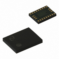
LMX2332USLBX National Semiconductor, LMX2332USLBX Datasheet - Page 32

LMX2332USLBX
Manufacturer Part Number
LMX2332USLBX
Description
IC FREQ SYNTH DUAL 24LAMINATECSP
Manufacturer
National Semiconductor
Series
PLLatinum™r
Type
PLL Frequency Synthesizerr
Datasheet
1.LMX2330UTM.pdf
(49 pages)
Specifications of LMX2332USLBX
Pll
Yes with Bypass
Input
CMOS, TTL
Output
CMOS
Number Of Circuits
1
Ratio - Input:output
3:1
Differential - Input:output
Yes/No
Frequency - Max
1.2GHz, 600MHz
Divider/multiplier
Yes/No
Voltage - Supply
2.7 V ~ 5.5 V
Operating Temperature
-40°C ~ 85°C
Mounting Type
Surface Mount
Package / Case
24-Laminate CSP
Frequency-max
1.2GHz
Lead Free Status / RoHS Status
Contains lead / RoHS non-compliant
Other names
LMX2332USLBXTR
www.national.com
Test Setups
The block diagram above illustrates the setup required to
measure the LMX233xU device’s RF charge pump sink cur-
rent. The same setup is used for the LMX2330TMEB/
LMX2330SLEEB Evaluation Boards. The IF charge pump
measurement setup is similar to the RF charge pump mea-
surement setup. The purpose of this test is to assess the
functionality of the RF charge pump.
This setup uses an open loop configuration. A power supply
is connected to V
of a signal generator, a 10 MHz signal is typically applied to
the f
detector. The 3 dB pad provides a 50 Ω match between the
PLL and the signal generator. The OSC
This establishes the other input to the phase detector. Alter-
natively, this input can be tied directly to the ground plane.
With the D
eter Analyzer in this way, the sink, source, and TRI-STATE
currents can be measured by simply toggling the Phase
Detector Polarity and Charge Pump State states in Code
Loader. Similarly, the LOW and HIGH currents can be mea-
IN
RF pin. The signal is one of two inputs to the phase
o
RF pin connected to a Semiconductor Param-
cc
and swept from 2.7V to 5.5V. By means
in
pin is tied to V
LMX233xU Charge Pump Test Setup
cc
.
32
sured by switching the Charge Pump Gain’s state between
1X and 4X in Code Loader.
Let F
OSC
represent the frequency of the signal applied to the f
pin. The phase detector is sensitive to the rising edges of F
and F
pump turns ON and sinks current when the first rising edge
of F
pump continues to sink current indefinitely.
Toggling the Phase Detector Polarity state to negative
VCO characteristics allows the measurement of the RF
charge pump source current. Likewise, selecting TRI-STATE
(TRI-STATE ID
Loader facilitates the measurement of the TRI-STATE cur-
rent.
The measurements are repeated at different temperatures,
namely T
p
in
r
p
is detected. Since F
represent the frequency of the signal applied to the
pin, which is simply zero in this case (DC), and let F
. Assuming positive VCO characteristics; the charge
A
= -40˚C, +25˚C, and +85˚C.
o
RF Bit = 1) for Charge Pump State in Code
r
has no rising edge, the charge
10136650
IN
RF
p
r


