SI5364-G-BC Silicon Laboratories Inc, SI5364-G-BC Datasheet - Page 10
SI5364-G-BC
Manufacturer Part Number
SI5364-G-BC
Description
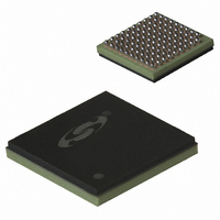
IC PREC PORT CARD CLOCK 99CBGA
Manufacturer
Silicon Laboratories Inc
Type
Clock Generatorr
Datasheet
1.SI5364-H-GL.pdf
(38 pages)
Specifications of SI5364-G-BC
Package / Case
99-CBGA
Pll
Yes
Input
Clock
Output
CML
Number Of Circuits
1
Ratio - Input:output
3:4
Differential - Input:output
Yes/Yes
Frequency - Max
675MHz
Divider/multiplier
No/Yes
Voltage - Supply
3.135 V ~ 3.465 V
Operating Temperature
-20°C ~ 85°C
Mounting Type
Surface Mount
Frequency-max
675MHz
Mounting Style
SMD/SMT
Operating Supply Voltage
2.3 V to 3.3 V
Lead Free Status / RoHS Status
Contains lead / RoHS non-compliant
Other names
336-1280
Available stocks
Company
Part Number
Manufacturer
Quantity
Price
Company:

Part Number:
SI5364-G-BC
Manufacturer:
LATTICE
Quantity:
190
Company:
Part Number:
SI5364-G-BC
Manufacturer:
SILICON
Quantity:
748
Company:
Part Number:
SI5364-G-BC
Manufacturer:
Silicon Laboratories Inc
Quantity:
10 000
Part Number:
SI5364-G-BC
Manufacturer:
SILICON LABS/芯科
Quantity:
20 000


Table 4. AC Characteristics (PLL Performance Characteristics) (Continued)
(V
Si5364
10
CLKOUT RMS Jitter Generation
FEC[1:0] = 01, 10 (255/238, 238/255 Scal-
ing)
CLKOUT Peak-Peak Jitter Generation
FEC[1:0] = 00 (1/1 Scaling)
CLKOUT Peak-Peak Jitter Generation
FEC[1:0] = 01, 10 (255/238, 238/255 Scal-
ing)
Jitter Transfer Bandwidth (See Figure 9)
Wander/Jitter Transfer Peaking
Wander/Jitter at 1600 Hz Bandwidth
(BWSEL[1:0] = 01)
Jitter Tolerance (see Figure 8)
CLKOUT RMS Jitter Generation
FEC[1:0] = 00
CLKOUT RMS Jitter Generation
FEC[1:0] = 01, 10
CLKOUT Peak-Peak Jitter Generation
FEC[1:0] = 00
CLKOUT Peak-Peak Jitter Generation
FEC[1:0] = 01, 10
Jitter Transfer Bandwidth (see Figure 9 )
Wander/Jitter Transfer Peaking
Wander/Jitter at 3200 Hz Bandwidth
(BWSEL[1:0] = 00)
Jitter Tolerance (see Figure 8)
CLKOUT RMS Jitter Generation
FEC[1:0] = 00 (1/1 Scaling)
CLKOUT RMS Jitter Generation
FEC[1:0] = 01, 10 (255/238, 238/255 Scal-
ing)
CLKOUT Peak-Peak Jitter Generation
FEC[1:0] = 00 (1/1 Scaling)
Notes:
DD33
1. Higher PLL bandwidth settings provide smaller clock output wander with temperature gradient.
2. For reliable device operation, temperature gradients should be limited to 10 °C/min.
3. Telcordia GR-1244-CORE requirements specify maximum phase transient slope during clock rearrangement in terms
= 3.3 V ± 5%, TA = –20 to 85 °C)
of nanoseconds per millisecond. The equivalent ps/ μ s unit is used here since the maximum phase transient magnitude
for the Si5364 (t
Parameter
PT_MTIE
) never reaches one nanosecond.
J
J
J
J
J
J
J
J
J
J
Symbol
J
GEN(RMS)
GEN(RMS)
J
GEN(RMS)
GEN(RMS)
GEN(RMS)
GEN(PP)
GEN(PP)
GEN(PP)
GEN(PP)
GEN(PP)
TOL(PP)
TOL(PP)
F
F
J
J
BW
BW
P
P
Rev. 2.5
12 kHz to 20 MHz
50 kHz to 80 MHz
12 kHz to 20 MHz
50 kHz to 80 MHz
12 kHz to 20 MHz
50 kHz to 80 MHz
12 kHz to 20 MHz
50 kHz to 80 MHz
12 kHz to 20 MHz
50 kHz to 80 MHz
12 kHz to 20 MHz
50 kHz to 80 MHz
12 kHz to 20 MHz
50 kHz to 80 MHz
12 kHz to 20 MHz
50 kHz to 80 MHz
12 kHz to 20 MHz
50 kHz to 80 MHz
12 kHz to 20 MHz
50 kHz to 80 MHz
Test Condition
BW = 1600 Hz
BW = 800 Hz
f = 1600 Hz
f = 3200 Hz
f = 160 Hz
< 1600 Hz
f = 320 Hz
< 800 Hz
f = 16 Hz
f = 32 Hz
1000
1000
Min
100
100
10
10
—
—
—
—
—
—
—
—
—
—
—
—
—
—
—
—
—
—
—
—
—
—
—
—
1600
0.86
0.26
0.83
0.26
0.26
0.89
0.81
0.30
Typ
800
6.1
2.1
6.0
2.0
0.0
0.8
5.7
2.0
5.4
1.9
0.0
0.3
5.8
2.9
—
—
—
—
—
—
Max Unit
0.35
10.0
10.0
0.05
0.35
0.35
10.0
1.2
5.0
5.0
1.0
1.0
9.0
5.0
9.0
5.0
0.1
1.2
0.4
1.2
0.4
5.0
—
—
—
—
—
—
—
—
Hz
dB
Hz
dB
ps
ps
ps
ps
ps
ps
ns
ns
ns
ps
ps
ps
ps
ps
ps
ps
ps
ns
ns
ns
ps
ps
ps
ps
ps
ps
Related parts for SI5364-G-BC
Image
Part Number
Description
Manufacturer
Datasheet
Request
R

Part Number:
Description:
IC CLOCK SONET/SDH PORT 99LFBGA
Manufacturer:
Silicon Laboratories Inc
Datasheet:

Part Number:
Description:
IC PREC PORT CARD CLOCK 99CBGA
Manufacturer:
Silicon Laboratories Inc
Datasheet:
Part Number:
Description:
IC CLK MULT SONET/SDH 99-PBGA
Manufacturer:
Silicon Laboratories Inc
Datasheet:
Part Number:
Description:
BOARD EVALUATION FOR SI5364
Manufacturer:
Silicon Laboratories Inc
Datasheet:
Part Number:
Description:
SMD/C°/SINGLE-ENDED OUTPUT SILICON OSCILLATOR
Manufacturer:
Silicon Laboratories Inc
Part Number:
Description:
Manufacturer:
Silicon Laboratories Inc
Datasheet:
Part Number:
Description:
N/A N/A/SI4010 AES KEYFOB DEMO WITH LCD RX
Manufacturer:
Silicon Laboratories Inc
Datasheet:
Part Number:
Description:
N/A N/A/SI4010 SIMPLIFIED KEY FOB DEMO WITH LED RX
Manufacturer:
Silicon Laboratories Inc
Datasheet:
Part Number:
Description:
N/A/-40 TO 85 OC/EZLINK MODULE; F930/4432 HIGH BAND (REV E/B1)
Manufacturer:
Silicon Laboratories Inc
Part Number:
Description:
EZLink Module; F930/4432 Low Band (rev e/B1)
Manufacturer:
Silicon Laboratories Inc
Part Number:
Description:
I°/4460 10 DBM RADIO TEST CARD 434 MHZ
Manufacturer:
Silicon Laboratories Inc
Part Number:
Description:
I°/4461 14 DBM RADIO TEST CARD 868 MHZ
Manufacturer:
Silicon Laboratories Inc
Part Number:
Description:
I°/4463 20 DBM RFSWITCH RADIO TEST CARD 460 MHZ
Manufacturer:
Silicon Laboratories Inc
Part Number:
Description:
I°/4463 20 DBM RADIO TEST CARD 868 MHZ
Manufacturer:
Silicon Laboratories Inc