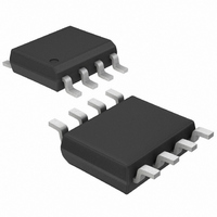
DS1100Z-250+ Maxim Integrated Products, DS1100Z-250+ Datasheet

DS1100Z-250+
Specifications of DS1100Z-250+
Related parts for DS1100Z-250+
DS1100Z-250+ Summary of contents
Page 1
... Custom Delays Available Fast-Turn Prototypes Delays Specified Over Both Commercial and Industrial Temperature Ranges PIN ASSIGNMENT IN 1 TAP 2 2 TAP 4 3 GND 4 DS1100Z SO (150 mils) DS1100U µMAX® PIN DESCRIPTION TAP 1 to TAP 5 - TAP Output Number V - +5V CC GND - Ground IN - Input 19-5735 ...
Page 2
ABSOLUTE MAXIMUM RATINGS Voltage Range on Any Pin Relative to Ground ........................... -0.5V to +6.0V Short-Circuit Output Current ...................................................... 50mA for 1s Operating Temperature Range .................................................... -40°C to +85°C Storage Temperature Range ........................................................ -55°C to +125°C Lead Temperature (soldering, 10s) ...
Page 3
NOTES: 1) Initial tolerances are ± with respect to the nominal value at +25°C and 5V for both leading and trailing edge. 2) Temperature and voltage tolerance is with respect to the nominal delay value over the stated temperature range, ...
Page 4
TERMINOLOGY Period: The time elapsed between the leading edge of the first pulse and the leading edge of the following pulse. t (Pulse Width): The elapsed time on the pulse between the 1.5V point on the leading edge and the ...
Page 5
Figure 3. TEST CIRCUIT Table 1. DS1100 PART NUMBER DELAY PART DS1100-xxx TAP 1 -20 4 -25 5 -30 6 -35 7 -40 8 -45 9 -50 10 -60 12 -75 15 -100 20 -125 25 -150 30 -175 35 ...
Page 6
... ORDERING INFORMATION PART DS1100Z-xxx DS1100Z-xxx/T&R DS1100Z-xxx+ DS1100Z-xxx+T DS1100U-xxx DS1100U-xxx/T&R DS1100U-xxx+ DS1100U-xxx+T xxx Denotes total time delay (ns) (see Table 1). +Denotes a lead(Pb)-free/RoHS-compliant package. T&R and T = Tape and reel. PACKAGE INFORMATION For the latest package outline information and land patterns (footprints www.maxim-ic.com/packages. Note that a “+”, “ ...
Page 7
... Maxim cannot assume responsibility for use of any circuitry other than circuitry entirely embodied in a Maxim product. No circuit patent licenses are implied. Maxim reserves the right to change the circuitry and specifications without notice at any time 2011 Maxim Integrated Products DESCRIPTION Maxim is a registered trademark of Maxim Integrated Products. DS1100 PAGES CHANGED 1−6 ...


