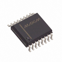
DS1023S-25+ Maxim Integrated Products, DS1023S-25+ Datasheet

DS1023S-25+
Specifications of DS1023S-25+
Related parts for DS1023S-25+
DS1023S-25+ Summary of contents
Page 1
... Combined with an on-chip reference delay (to offset the inherent or “step zero” delay of the device) clock phase can now be varied over the full 0-360 degree range. 8-Bit Programmable Timing Element PIN ASSIGNMENT Q/P0 3 CLK/ GND 8 DS1023 300-mil DIP DS1023S 300-mil SOIC PIN DESCRIPTION IN P0/Q P1/CLK P2 GND OUT/ OUT REF/PWM / DS1023 V 16 ...
Page 2
On-chip gating is provided to allow the device to provide a pulse width modulated output, triggered by the input with duration set by the programmed value. Alternatively the output signal may be inverted on chip, allowing the device to perform ...
Page 3
Applications can read the setting of the DS1023 Delay Line by connecting the serial output pin (Q) to the serial input (D) through a resistor with a value kohms (Figure 2). Since the read process is ...
Page 4
For highest accuracy it is strongly recommended that the reference delay is used. Variations in input voltage levels and transition times can significantly alter the measured delay from input to output. This effect is totally removed if the reference delay ...
Page 5
Figure 4 Output Function Pulse Width Modulated Output Delayed and Inverted Output PWM is an output triggered by the rising edge of the input waveform. After a time interval approximately equal to the Step Zero delay of ...
Page 6
FUNCTIONAL BLOCK DIAGRAM Figure 5 DELAY LINE DETAIL (CONCEPTUAL) - DS1023-200, DS1023-500 Figure ...
Page 7
DELAY LINE DETAIL (CONCEPTUAL) - DS1023-25, DS1023-50, DS1023-100 Figure 7 PART NUMBER TABLE Table 1 DELAYS RANGES AND TOLERANCE (all times measured in ns) MAX. DELAY TIME (1)/ PART STEP MAX. OUTPUT PULSE NUMBER SIZE DS1023-25 0.25 DS1023-50 0.50 DS1023-100 ...
Page 8
DALLAS SEMICONDUCTOR TEST CIRCUIT Figure 8 TEST SETUP DESCRIPTION Figure 8 illustrates the hardware configuration used for measuring the timing parameters of the DS1023. The input waveform is produced by a precision pulse generator under software control. Time delays are ...
Page 9
ABSOLUTE MAXIMUM RATINGS* Voltage on Any Pin Operating Temperature Range Storage Temperature Soldering Temperature Short Circuit Output Current * This is a stress rating only and functional operation of the device at these or any other conditions above those indicated ...
Page 10
TIMING DIAGRAM: SILICON DELAY LINE Figure 9 AC ELECTRICAL CHARACTERISTICS - DS1023-25 Delay Specifications PARAMETER Step Zero Delay -absolute -wrt REF Reference Delay Delay Step Size Maximum Delay -absolute -wrt REF Integral Non-linearity (deviation from straight line) Delta Delay OUT ...
Page 11
AC ELECTRICAL CHARACTERISTICS – DS1023-50 Delay Specifications PARAMETER Step Zero Delay -absolute -wrt REF Reference Delay Delay Step Size Maximum Delay -absolute -wrt REF Integral Non-linearity (deviation from straight line) Delta Delay OUT IN High to PWM High Minimum PWM ...
Page 12
AC ELECTRICAL CHARACTERISTICS - DS1023-200 Delay Specifications PARAMETER Step Zero Delay -absolute -wrt REF Reference Delay Delay Step Size Maximum Delay -absolute -wrt REF Integral Non- linearity (deviation from straight line) Delta Delay OUT IN High to PWM High Minimum ...
Page 13
NOTES: 1. Delay from input to output with a programmed delay value of zero. 2. This is the relative delay between REF and OUT. The device is trimmed such that when programmed to zero delay the OUT output will always ...
Page 14
TERMINOLOGY Period: The time elapsed between the leading edge of the first pulse and the leading edge of the following pulse. t (Pulse Width): The elapsed time on the pulse between the 1.5V point on the leading edge and the ...
Page 15
TIMING DIAGRAM: SERIAL MODE ( DELAY vs PROGRAMMED VALUE Figure 13 t DMAX (measured Figure ...
Page 16
DETAILED RESPONSE CHARACTERISTICS Figure 14 DELAY PARAMETERS Figure 15 NOTES: 1. The device is trimmed such that t 2. Since t is trimmed to be less than Consequently the range of absolute delay values (t amount equal ...


