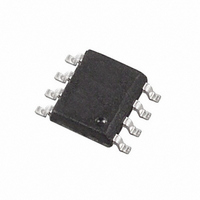
ZSCT1555N8TA Diodes Zetex, ZSCT1555N8TA Datasheet - Page 7

ZSCT1555N8TA
Manufacturer Part Number
ZSCT1555N8TA
Description
IC TIMER PRECISION 555 8-SOIC
Manufacturer
Diodes Zetex
Type
555 Type, Timer/Oscillator (Single)r
Datasheet
1.ZSCT1555N8TA.pdf
(11 pages)
Specifications of ZSCT1555N8TA
Frequency
330kHz
Voltage - Supply
0.9 V ~ 6 V
Current - Supply
150µA
Operating Temperature
-20°C ~ 100°C
Package / Case
8-SOIC (3.9mm Width)
# Internal Timers
1
Power Dissipation
625mW
Operating Supply Voltage (min)
0.9V
Operating Supply Voltage (typ)
1.5V
Operating Supply Voltage (max)
6V
Package Type
SOIC
Low Level Output Current
100mA
Pin Count
8
Operating Temperature Classification
Commercial
Mounting
Surface Mount
Lead Free Status / RoHS Status
Lead free / RoHS Compliant
Count
-
Lead Free Status / RoHS Status
Lead free / RoHS Compliant, Compliant
Other names
ZSCT1555N8TR
Available stocks
Company
Part Number
Manufacturer
Quantity
Price
Company:
Part Number:
ZSCT1555N8TA
Manufacturer:
Diodes/Zetex
Quantity:
1 990
Issue 3 - July 2006
© Zetex Semiconductors plc 2006
APPLICATIONS INFORMATION
Many configurations of the ZSCT1555 are
possible. The following gives a selection of a
few of these using the most basic monostable
and astable connections. The final application
example in astable mode shows the device
optimum use for low voltage and power
economy in a single cell boost converter.
Monostable Operation
Figure 1 shows connection of the timer as a
one-shot whose pulse period is independent
of supply voltage. Initially the capacitor is held
discharged. The application of a negative
going trigger pulse sets an internal flip flop
which allows the capacitor to start to charge
up via RA and forces the output high. The
voltage on the capacitor increases for time t,
where t = 1.63RAC
the voltage on the capacitor is 0.8 V
point the flip flop resets, the capacitor is
discharged and the output is driven low.
Figure 2 shows the timing diagram for this
function. During the output high period
further trigger pulses are locked out however
the circuit can be reset by application of a
negative going pulse on the reset pin. Once
the output is driven low it remains in this state
until the application of the next trigger pulse.
If the reset function is not used then it is
recommended to connect to V
any possibility of false triggering.
Figure 1
T
, at the end of this period
CC
to eliminate
CC
. At this
Figure 3 gives an easy selection of RA and C
values for various time delays.
This configuration of circuit can be used as a
frequency divider by adjusting the timing
period. Figure 4 indicates a divide by three.
Figure 3
Figure 4
0.001
Figure 2
0.01
100
0.1
10
1
10us 100us 1ms
R
A
Time Delay
ZSCT1555
10ms 100ms 1s
www.zetex.com
100k
10M
1M
10s
T


