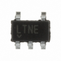
LTC1799IS5#TRMPBF Linear Technology, LTC1799IS5#TRMPBF Datasheet

LTC1799IS5#TRMPBF
Specifications of LTC1799IS5#TRMPBF
Available stocks
Related parts for LTC1799IS5#TRMPBF
LTC1799IS5#TRMPBF Summary of contents
Page 1
... Small Footprint Replacement for Econ Oscillators n L, LT, LTC, LTM, Linear Technology and the Linear logo are registered trademarks and ThinSOT is a trademark of Linear Technology Corporation. All other trademarks are the property of their respective owners. Protected by U.S. Patents including 6342817 and 6614313. Typical applicaTion ...
Page 2
LTC1799 absoluTe MaxiMuM raTings (Note 1) + Supply Voltage ( GND ......................... –0. DIV to GND .....................................–0. SET to GND .....................................–0. Operating Temperature Range LTC1799C ................................................ 0°C to 70°C LTC1799I .............................................–40°C to ...
Page 3
T voltages are with respect to GND. SYMBOL PARAMETER Duty Cycle (Note Operating Supply Range I Power Supply Current S V High Level DIV Input Voltage IH V Low ...
Page 4
LTC1799 Typical perForMance characTerisTics Frequency Variation vs R SET 25°C A GUARANTEED LIMITS APPLY 3 OVER 5k TO 200k RANGE –1 –2 –3 – SET Peak-to-Peak Jitter vs Frequency 0.7 0.6 ...
Page 5
FuncTions + V (Pin 1): Voltage Supply (2.7V ≤ V ply must be kept free from noise and ripple. It should be bypassed directly to a ground plane with a 0.1µF capacitor. GND (Pin 2): Ground. Should be tied ...
Page 6
LTC1799 Theory oF operaTion As shown in the Block Diagram, the LTC1799’s master oscillator is controlled by the ratio of the voltage between + the V and SET pins and the current entering the SET pin (I ). The voltage ...
Page 7
SELECTING THE DIVIDER SETTING AND RESISTOR The LTC1799’s master oscillator has a frequency range spanning 0.1MHz to 33MHz. However, accuracy may suffer if the master oscillator is operated at greater than 10MHz with a supply voltage lower than ...
Page 8
LTC1799 applicaTions inForMaTion POwER SUPPLY REJECTION Low Frequency Supply Rejection (Voltage Coefficient) Figure 5 shows the output frequency sensitivity to power supply voltage at several different temperatures. The LTC1799 has a conservative guaranteed voltage coeffi- cient of 0.1%/V but, as ...
Page 9
Jitter The typical jitter is listed in the Electrical Characteristics and shown in the Typical Performance Characteristics. These specifications assume that the capacitance on SET (Pin 3) is limited to less than 10pF , as suggested in the ...
Page 10
LTC1799 applicaTions inForMaTion Once known, calculate R IN SET 10MHz 10k R = • • SET N f OSC(MAX − IN(MAX) RES R ...
Page 11
Typical applicaTion Low Power 80Hz to 8kHz Sine wave Generator ( OSC OUT 3V LTC1799 SET 3V 100 0.1µF GND SW1 OPEN SET DIV ...
Page 12
LTC1799 package DescripTion 0.62 MAX 3.85 MAX 2.62 REF RECOMMENDED SOLDER PAD LAYOUT PER IPC CALCULATOR 0.20 BSC DATUM ‘A’ 0.30 – 0.50 REF NOTE: 1. DIMENSIONS ARE IN MILLIMETERS 2. DRAWING NOT TO SCALE 3. DIMENSIONS ARE INCLUSIVE OF ...
Page 13
... Revised part number in Maximum VCO Modulation Bandwidth section. Information furnished by Linear Technology Corporation is believed to be accurate and reliable. However, no responsibility is assumed for its use. Linear Technology Corporation makes no representa- tion that the interconnection of its circuits as described herein will not infringe on existing patent rights. ...
Page 14
... OSC 800 600 4 400 1799 TA03 200 www.linear.com ● 5 OUT OUT 4 DIV 1799 TA08 Output Frequency vs Temperature MAX TYP MIN 0 –20 – TEMPERATURE (°C) 1799 TA04 LT 0111 REV C • PRINTED IN USA LINEAR TECHNOLOGY CORPORA TION 2001 1799fc ...


