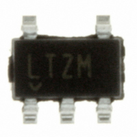
LTC6900IS5#TRMPBF Linear Technology, LTC6900IS5#TRMPBF Datasheet - Page 5

LTC6900IS5#TRMPBF
Manufacturer Part Number
LTC6900IS5#TRMPBF
Description
IC OSC PREC LP RES SET TSOT23-5
Manufacturer
Linear Technology
Type
Oscillator, Siliconr
Datasheet
1.LTC6900CS5TRMPBF.pdf
(12 pages)
Specifications of LTC6900IS5#TRMPBF
Frequency
20MHz
Voltage - Supply
2.7 V ~ 5.5 V
Current - Supply
920µA
Operating Temperature
-40°C ~ 85°C
Package / Case
TSOT-23-5, TSOT-5, TSOP-5
Lead Free Status / RoHS Status
Lead free / RoHS Compliant
Count
-
Other names
LTC6900IS5#PBF
LTC6900IS5#PBF
LTC6900IS5#TRMPBF
LTC6900IS5#TRMPBFTR
LTC6900IS5#PBF
LTC6900IS5#TRMPBF
LTC6900IS5#TRMPBFTR
Available stocks
Company
Part Number
Manufacturer
Quantity
Price
PIN FUNCTIONS
V
must be kept free from noise and ripple. It should be by-
passed directly to a ground plane with a 0.1μF capacitor.
GND (Pin 2): Ground. Should be tied to a ground plane
for best performance.
SET (Pin 3): Frequency-Setting Resistor Input. The value
of the resistor connected between this pin and V
mines the oscillator frequency. The voltage on this pin is
held by the LTC6900 to approximately 1.1V below the V
voltage. For best performance, use a precision metal fi lm
resistor with a value between 10kΩ and 2MΩ and limit
the capacitance on this pin to less than 10pF .
DIV (Pin 4): Divider-Setting Input. This three-state input
selects among three divider settings, determining the value
of N in the frequency equation. Pin 4 should be tied to GND
BLOCK DIAGRAM
+
(Pin 1): Voltage Supply (2.7V ≤ V
R
SET
I
RES
1
3
2
PATENT PENDING
GND
V
SET
+
V
BIAS
I
RES
V
+
–
RES
GAIN = 1
= (V
+
+
≤ 5.5V). This supply
– V
SET
) = 1.1V TYPICALLY
ƒ
MO
= 10MHz • 20kΩ •
+
MASTER OSCILLATOR
deter-
+
(V
for the ÷1 setting, the highest frequency range. Floating
Pin 4 divides the master oscillator by 10. Pin 4 should be
tied to V
To detect a fl oating DIV pin, the LTC6900 attempts to pull
the pin toward midsupply. Therefore, driving the DIV pin
high requires sourcing approximately 2μA. Likewise, driv-
ing DIV low requires sinking 2μA. When Pin 4 is fl oated,
it should preferably be bypassed by a 1nF capacitor to
ground or it should be surrounded by a ground shield to
prevent excessive coupling from other PCB traces.
OUT (Pin 5): Oscillator Output. This pin can drive 5kΩ and/
or 10pF loads. Heavier loads may cause inaccuracies due
to supply bounce at high frequencies. Voltage transients,
coupled into Pin 5, above or below the LTC6900 power
supplies will not cause latchup if the current into/out of
the OUT pin is limited to 50mA.
+
I
– V
RES
SET
)
+
for the ÷100 setting, the lowest frequency range.
DIVIDER
SELECT
PROGRAMMABLE
(÷1, 10 OR 100)
INPUT DETECT
THREE-STATE
DIVIDER (N)
+
–
+
–
GND
LTC6900
OUT
2μA
2μA
DIV
V
6900 BD
+
5
4
6900fa
5


