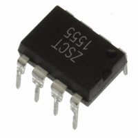
ZSCT1555D8 Diodes Zetex, ZSCT1555D8 Datasheet

ZSCT1555D8
Specifications of ZSCT1555D8
Related parts for ZSCT1555D8
ZSCT1555D8 Summary of contents
Page 1
PRECISION SINGLE CELL TIMER ISSUE 3 - JULY 2006 DEVICE DESCRIPTION These devices are precision timing circuits for generation of accurate time delays or oscillation. Advanced circuit design means that these devices can operate from a single battery cell with ...
Page 2
ZSCT1555 ABSOLUTE MAXIMUM RATINGS Supply Voltage Input Voltages (Cont, Reset, Thres, Trig) Output Current Operating Temperature Storage Temperature ELECTRICAL CHARACTERISTICS TEST CONDITIONS (Unless otherwise stated):T SYMBOL PARAMETER V Supply Voltage CC I Supply Current CC V Threshold Voltage TH I ...
Page 3
ELECTRICAL CHARACTERISTICS (Continued) TEST CONDITIONS (Unless otherwise stated):T SYMBOL PARAMETER t Output pulse rise time R t Output pulse fall time F Timing error, Monostable Initial accuracy (Note 2) t (m) IA Drift with supply voltage t (m) V Drift ...
Page 4
ZSCT1555 +100°C 2 +25°C -20° Lowest Voltage Level of Trigger Pulse (xVcc) Minimum Pulse Width Required for Triggering 5 4 +100°C 3 +25°C -20° Lowest Voltage Level of Trigger Pulse ...
Page 5
Vcc=1.5v 0.8 0.6 -20°C 0.4 +25°C +100°C 0.2 0.0 0.001 0.01 High-Level Output Current (mA) Output High Voltage Drop v Output Current 2.0 Vcc=1.5v 1.8 1.6 1.4 1.2 1.0 0.8 0.6 0.4 0.2 0.0 0.01 0.1 Low Level Output ...
Page 6
ZSCT1555 FUNCTIONAL DIAGRAM FUNCTIONAL TABLE RESET TRIGGER VALUE THRESHOLD Low N/A High < High > High > POWER DERATING TABLE Package TA 25°C Power Rating N8 625mW D8 625mW Issue 3 - July 2006 ...
Page 7
APPLICATIONS INFORMATION Many configurations of the ZSCT1555 are possible. The following gives a selection of a few of these using the most basic monostable and astable connections. The final application example in astable mode shows the device optimum use for ...
Page 8
ZSCT1555 Figure 5 shows the monostable mode used as a pulse width modulator. Here the trigger pin is supplied with a continuous pulse train, the resulting output pulse width is modulated by a signal applied to the control pin. Figure ...
Page 9
Figure 9 gives an easy selection for RA, RB and C values. T 100 100k 10M 0.1 0.01 (RA+2RB) 0.001 0 Free Running Frequency (Hz) Figure 9 Similar to the PWM circuit of Figure 5 ...
Page 10
ZSCT1555 The circuit of Figure 12 shows the device in astable mode operating as part of a single cell boost converter. This circuit generates a 5 volt supply from a single battery cell. The circuit output voltage is maintained down ...
Page 11
Europe Americas Zetex GmbH Zetex Inc Streitfeldstraße 19 700 Veterans Memorial Highway D-81673 München Hauppauge, NY 11788 Germany USA Telefon: (49 Telephone: (1) 631 360 2222 Fax: (49 Fax: (1) ...


