DS4M125D+33 Maxim Integrated Products, DS4M125D+33 Datasheet

IC OSC CLOCK 125MHZ 10-LCCC

DS4M125D+33

Manufacturer Part Number
DS4M125D+33
Description
IC OSC CLOCK 125MHZ 10-LCCC
Manufacturer
Maxim Integrated Products
Type
Clock Oscillatorr
Datasheet

Specifications of DS4M125D+33

Frequency
125MHz
Voltage - Supply
3.135 V ~ 3.465 V
Current - Supply
74mA
Operating Temperature
-40°C ~ 85°C
Package / Case
10-LCCC
Lead Free Status / RoHS Status
Lead free / RoHS Compliant
Count
-
The DS4M125/DS4M133/DS4M200 are margining clock
oscillators with LVPECL or LVDS outputs. They are
designed to fit in a 5mm x 3.2mm ceramic package with
an AT-cut fundamental-mode crystal to form a complete
clock oscillator. The circuit can generate the following
frequencies and their ±5% frequency deviations:
125MHz, 133.33MHz, and 200MHz. The DS4M125/
DS4M133/DS4M200 employ a low-jitter PLL to generate
the frequencies. The typical phase jitter is less than
0.9ps RMS from 12kHz to 20MHz.
Frequency margining is a circuit operation to change
the output frequency to 5% higher or 5% lower than the
nominal frequency. Frequency margining is accom-
plished through the margining select pin, MS. This
three-state input pin accepts a three-level voltage signal
to control the output frequency. In a low-level state, the
output frequency is set to the nominal frequency. When
set to a high-level state, the frequency output is set to
the nominal frequency plus 5%. When set to the mid-
level state, the frequency output is equal to the nominal
frequency minus 5%. If left open, the MS pin is pulled
low by an internal 100kΩ (nominal) pulldown resistor.
The DS4M125/DS4M133/DS4M200 are available with
either an LVPECL or LVDS output. The output can be
disabled by pulling the OE pin low. When disabled,
both OUTP and OUTN levels of the LVPECL driver go to
the LVPECL bias voltage, while the output of the LVDS
driver is a logical one. The OE input is an active-high
logic signal and has an internal 100kΩ pullup resistor.
When OE is in a logic-high state, the OUTP and OUTN
outputs are enabled.
The devices operate from a single 3.3V supply voltage.
Rev 0; 12/07
For pricing, delivery, and ordering information, please contact Maxim Direct at 1-888-629-4642,
or visit Maxim’s website at www.maxim-ic.com.
0.1μF
Memory Clocks
RAID Systems
0.01μF
________________________________________________________________ Maxim Integrated Products
General Description
3.3V Margining Clock Oscillator with
VCC
MS
OE
GND
LVDS OPTION
DS4M125/
DS4M133/
DS4M200
Applications
OUTN
OUTP
100Ω
0.1μF
♦ Frequency Margining: ±5%
♦ Nominal Clock Output Frequencies: 125MHz,
♦ Jitter < 0.9ps RMS from 12kHz to 20MHz
♦ LVPECL or LVDS Output
♦ 3.3V Operating Voltage
♦ Operating Temperature Range: -40°C to +85°C
♦ Supply Current: < 100mA at 3.3V
♦ Excellent Power-Supply Noise Rejection
♦ 5mm x 3.2mm Ceramic LCCC Package
♦ Output Enable/Disable
+ Denotes a lead(Pb)-free package. The lead finish is JESD97
category e4 (Au over Ni) and is compatible with both lead-based
and lead-free soldering processes.
Pin Configuration and Selector Guide appear at end of
data sheet.
DS4M125P+33
DS4M125D+33
DS4M133P+33
DS4M133D+33
DS4M200P+33
DS4M200D+33
133.33MHz, and 200MHz
0.01μF
LVPECL/LVDS Output
PART
Typical Operating Circuit
-40°C to +85°C
-40°C to +85°C
-40°C to +85°C
-40°C to +85°C
-40°C to +85°C
-40°C to +85°C
TEMP RANGE
MS
OE
GND
VCC
Ordering Information
LVPECL OPTION
DS4M125/
DS4M133/
DS4M200
OUTN
OUTP
PIN-PACKAGE
10 LCCC
10 LCCC
10 LCCC
10 LCCC
10 LCCC
10 LCCC
50Ω
50Ω
Features
PECL_BIAS AT
V
CC
- 2.0V
1

Related parts for DS4M125D+33

DS4M125D+33 Summary of contents

Page 1

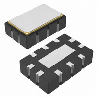
... Supply Current: < 100mA at 3.3V ♦ Excellent Power-Supply Noise Rejection ♦ 5mm x 3.2mm Ceramic LCCC Package ♦ Output Enable/Disable PART DS4M125P+33 DS4M125D+33 DS4M133P+33 DS4M133D+33 DS4M200P+33 DS4M200D+33 + Denotes a lead(Pb)-free package. The lead finish is JESD97 category e4 (Au over Ni) and is compatible with both lead-based and lead-free soldering processes ...

Page 2

Margining Clock Oscillator with LVPECL/LVDS Output ABSOLUTE MAXIMUM RATINGS Power-Supply Voltage Range (V ) .....................-0.3V to +4.0V CC Continuous Power Dissipation (T = +70°C) ...................330mW A Operating Temperature Range ...........................-40°C to +85°C Junction Temperature ......................................................+125°C Stresses beyond those listed ...

Page 3

Margining Clock Oscillator with ELECTRICAL CHARACTERISTICS (continued 3.135V to 3.465V -40°C to +85°C, unless otherwise noted.) (Notes PARAMETER Input-Voltage Low (OE) Input-Leakage High (OE) Input-Leakage Low (OE) Input-Leakage High (MS) Input-Leakage ...

Page 4

Margining Clock Oscillator with LVPECL/LVDS Output ELECTRICAL CHARACTERISTICS (continued 3.135V to 3.465V -40°C to +85°C, unless otherwise noted.) (Notes PARAMETER LVPECL Output High Voltage (Note 2) Output Low Voltage (Note 2) ...

Page 5

Margining Clock Oscillator with PIN NAME 1 OE Active-High Output Enable. Has an internal pullup 100k 2 MS Margin Select. Three-level input with a 100k 3 GND Ground 4 OUTP Positive Output for LVPECL or LVDS 5 OUTN Negative ...

Page 6

Margining Clock Oscillator with LVPECL/LVDS Output X1 THREE- STATE X2 PHASE DET DS4M125/ DS4M133/ DS4M200 THREE- MS LEVEL DECODER GND Figure 1. Functional Diagram Detailed Description The DS4M125/DS4M133/DS4M200 consist of an oscil- lator designed to oscillate with a fundamental-mode ...

Page 7

... Margining Clock Oscillator with Selector Guide FREQUENCY OUTPUT PART (NOM) (MHz) TYPE DS4M125P+33 125 LVPECL DS4M125D+33 125 LVDS DS4M133P+33 133.33 LVPECL DS4M133D+33 133.33 LVDS DS4M200P+33 200 LVPECL DS4M200D+33 200 LVDS + Denotes a lead-free package. The lead finish is JESD97 cate- gory e4 (Au over Ni) and is compatible with both lead-based and lead-free soldering processes ...

Related keywords