DS4266P+ Maxim Integrated Products, DS4266P+ Datasheet
DS4266P+
Specifications of DS4266P+


Related parts for DS4266P+


DS4266P+ Summary of contents
Page 1
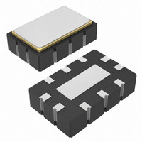
... Operating Temperature Range typically over a ♦ Lead-Free/RoHS Compliant PART DS4266D+ DS4266P+ + Denotes a lead(Pb)-free/RoHS-compliant package. The lead finish is JESD97 category e4 (Au over Ni) and is compatible with both lead-based and lead-free soldering processes. Pin Configuration and Selector Guide appear at end of data sheet ...
Page 2
DDR Clock Oscillator ABSOLUTE MAXIMUM RATINGS Power-Supply Voltage (V ) .......................................-0.3V, +4V CC Operating Temperature Range ...........................-40°C to +85°C Junction Temperature ......................................................+150°C Stresses beyond those listed under “Absolute Maximum Ratings” may cause permanent damage to the device. These are stress ...
Page 3
ELECTRICAL CHARACTERISTICS (continued 3.135V to 3.465V -40°C to +85°C, unless otherwise noted PARAMETER SYMBOL LVDS Output High Voltage V Output Low Voltage Differential Output Voltage Output Common-Mode Voltage V Variation Change ...
Page 4
DDR Clock Oscillator Single-Sideband Phase Noise 10Hz 100Hz 1kHz 10kHz 100kHz 1MHz 10MHz 20MHz (V = +3.3V +25°C, unless otherwise noted FREQUENCY vs. TEMPERATURE ...
Page 5
X1 THREE- STATE X2 PHASE DET DS4266 Figure 1. Functional Diagram Detailed Description The DS4266 consists of a fundamental-mode crystal and synthesizer IC packaged in a 5mm x 3.2mm x 1.49mm, 10-pin LCCC ceramic package. The device produces a frequency ...
Page 6
... DDR Clock Oscillator FREQUENCY (NOM) PART (MHz) DS4266D+ 266 DS4266P+ 266 + Denotes a lead(Pb)-free/RoHS-compliant package. The lead finish is JESD97 category e4 (Au over Ni) and is compatible with both lead-based and lead-free soldering processes. Pin Configuration TOP VIEW N.C. N. N.C. 2 DS4266 GND 3 *EP N.C. ...