LM555CJ National Semiconductor, LM555CJ Datasheet - Page 5
LM555CJ
Manufacturer Part Number
LM555CJ
Description
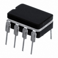
IC TIMER 8CDIP
Manufacturer
National Semiconductor
Type
555 Type, Timer/Oscillator (Single)r
Datasheet
1.LM555J.pdf
(12 pages)
Specifications of LM555CJ
Voltage - Supply
4.5 V ~ 16 V
Current - Supply
10mA
Operating Temperature
0°C ~ 70°C
Package / Case
8-CDIP (0.300", 7.62mm)
Frequency
100kHz
Lead Free Status / RoHS Status
Contains lead / RoHS non-compliant
Count
-
Other names
*LM555CJ
Available stocks
Company
Part Number
Manufacturer
Quantity
Price
Company:

Part Number:
LM555CJ
Manufacturer:
NSC
Quantity:
5 510
Company:
Part Number:
LM555CJ
Manufacturer:
OKI
Quantity:
5 510


Typical Performance Characteristics
Applications Information
MONOSTABLE OPERATION
In this mode of operation, the timer functions as a one-shot
( Figure 1 ). The external capacitor is initially held discharged
by a transistor inside the timer. Upon application of a nega-
tive trigger pulse of less than 1/3 V
set which both releases the short circuit across the capacitor
and drives the output high.
The voltage across the capacitor then increases exponen-
tially for a period of t = 1.1 R
voltage equals 2/3 V
flip-flop which in turn discharges the capacitor and drives the
output to its low state. Figure 2 shows the waveforms gener-
ated in this mode of operation. Since the charge and the
threshold level of the comparator are both directly propor-
tional to supply voltage, the timing internal is independent of
supply.
FIGURE 1. Monostable
CC
. The comparator then resets the
A
C, at the end of which time the
CC
to pin 2, the flip-flop is
Discharge Transistor (Pin 7)
Voltage vs Sink Current
DS007851-5
(Continued)
5
V
TIME = 0.1 ms/DIV.
R
C = 0.01 µF
During the timing cycle when the output is high, the further
application of a trigger pulse will not effect the circuit so long
as the trigger input is returned high at least 10 µs before the
end of the timing interval. However the circuit can be reset
during this time by the application of a negative pulse to the
reset terminal (pin 4). The output will then remain in the low
state until a trigger pulse is again applied.
When the reset function is not in use, it is recommended that
it be connected to V
gering.
Figure 3 is a nomograph for easy determination of R, C val-
ues for various time delays.
NOTE: In monostable operation, the trigger should be driven
high before the end of timing cycle.
CC
A
= 9.1 k
= 5V
DS007851-27
FIGURE 2. Monostable Waveforms
Top Trace: Input 5V/Div.
Bottom Trace: Capacitor Voltage 2V/Div.
Middle Trace: Output 5V/Div.
CC
to avoid any possibility of false trig-
www.national.com
DS007851-6
Related parts for LM555CJ
Image
Part Number
Description
Manufacturer
Datasheet
Request
R

Part Number:
Description:
National Semiconductor [8-Bit D/A Converter]
Manufacturer:
National Semiconductor
Datasheet:
Part Number:
Description:
National Semiconductor [Media Coprocessor]
Manufacturer:
National Semiconductor
Datasheet:
Part Number:
Description:
Digitally Controlled Tone and Volume Circuit with Stereo Audio Power Amplifier, Microphone Preamp Stage and National 3D Sound
Manufacturer:
National Semiconductor
Datasheet:
Part Number:
Description:
Digitally Controlled Tone and Volume Circuit with Stereo Audio Power Amplifier, Microphone Preamp Stage and National 3D Sound
Manufacturer:
National Semiconductor
Datasheet:
Part Number:
Description:
AC97 Rev 2 Codec with Sample Rate Conversion and National 3D Sound
Manufacturer:
National Semiconductor
Part Number:
Description:
Manufacturer:
National Semiconductor
Datasheet:
Part Number:
Description:
Manufacturer:
National Semiconductor
Datasheet:
Part Number:
Description:
General Purpose, Low Voltage, Low Power, Rail-to-Rail Output Operational Amplifiers
Manufacturer:
National Semiconductor
Datasheet:
Part Number:
Description:
8-bit 20 MSPS flash A/D converter.
Manufacturer:
National Semiconductor
Datasheet:
Part Number:
Description:
Low Noise Quad Operational Amplifier
Manufacturer:
National Semiconductor
Datasheet:
Part Number:
Description:
Quad Differential Line Receivers
Manufacturer:
National Semiconductor
Datasheet:
Part Number:
Description:
Quad High Speed Trapezoidal? Bus Transceiver
Manufacturer:
National Semiconductor
Datasheet:
Part Number:
Description:
Dual Line Receiver
Manufacturer:
National Semiconductor
Datasheet:
Part Number:
Description:
TTL to 10k ECL Level Translator with Latch
Manufacturer:
National Semiconductor
Datasheet: