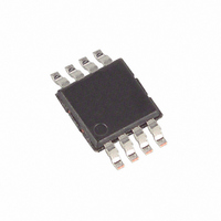
DS1337U+ Maxim Integrated Products, DS1337U+ Datasheet

DS1337U+
Specifications of DS1337U+
Related parts for DS1337U+
DS1337U+ Summary of contents
Page 1
... Operating Temperature Range CC ORDERING INFORMATION PART DS1337+ DS1337S+ DS1337U+ DS1337C# + Denotes a lead(Pb)-free/RoHS-compliant device. # Denotes a RoHS-compliant device that may include lead that is exempt under the RoHS requirements. The lead finish is JESD97 category e3, and is compatible with both lead-based and lead-free soldering processes. † ...
Page 2
ABSOLUTE MAXIMUM RATINGS Voltage Range on Any Pin Relative to Ground…………………………………………………………...…-0.3V to +6.0V Operating Temperature Range (Noncondensing)………………………………………………………….-40°C to +85°C Storage Temperature Range………………………………………………………………………………..-55°C to +125°C Soldering Temperature…………………………………………………………See IPC/JEDEC J-STD-020 Specification Stresses beyond those listed under “Absolute Maximum Ratings” may cause permanent ...
Page 3
AC ELECTRICAL CHARACTERISTICS (V = 1.8V to 5.5V -40°C to +85°C.) (Note PARAMETER SCL Clock Frequency Bus Free Time Between a STOP and START Condition Hold Time (Repeated) START Condition (Note 10) LOW Period of ...
Page 4
The parameter t is the period of time that the oscillator must be stopped for the OSF bit to be set over the Note 16: OSF voltage range of V CC(MIN) TYPICAL OPERATING CHARACTERISTICS (V = 3.3V +25°C, ...
Page 5
PIN DESCRIPTION PIN NAME — — X2 INTA GND 5 16 SDA 6 1 SCL 7 2 SQW/INTB — 4–13 N.C. TIMING DIAGRAM FUNCTION Connections for a ...
Page 6
BLOCK DIAGRAM "C" version only SERIAL BUS SCL INTERFACE AND ADDRESS REGISTER SDA DETAILED DESCRIPTION The Block Diagram shows the main elements of the DS1337. As shown, communications to and from the DS1337 2 ...
Page 7
CLOCK ACCURACY The accuracy of the clock is dependent upon the accuracy of the crystal and the accuracy of the match between the capacitive load of the oscillator circuit and the capacitive load for which the crystal was trimmed. Crystal ...
Page 8
ADDRESS MAP Table 2 shows the address map for the DS1337 registers. During a multibyte access, when the address pointer reaches the end of the register space (0Fh) it wraps around to location 00h pointer incrementing to ...
Page 9
CLOCK AND CALENDAR The time and calendar information is obtained by reading the appropriate register bytes. The RTC registers are illustrated in Table 2. The time and calendar are set or initialized by writing the appropriate register bytes. The contents ...
Page 10
Table 3. Alarm Mask Bits ALARM 1 REGISTER MASK BITS DY/DT (BIT 7) A1M4 A1M3 ALARM 2 REGISTER MASK BITS DY/DT (BIT ...
Page 11
Bit 1: Alarm 2 Interrupt Enable (A2IE). When set to logic 1, this bit permits the alarm 2 flag (A2F) bit in the status register to assert INTA (when INTCN = assert SQW/INTB (when INTCN = 1). ...
Page 12
I C SERIAL DATA BUS 2 The DS1337 supports the I C bus protocol. A device that sends data onto the bus is defined as a transmitter and a device receiving data as a receiver. The device that controls ...
Page 13
Figure 2. Data Transfer on I Depending upon the state of the R/W bit, two types of data transfer are possible: 1) Data transfer from a master transmitter to a slave receiver. The first byte transmitted by the master is ...
Page 14
Figure 3. Data Write—Slave Receiver Mode <Slave Address> <Word Address (n)> S 1101000 0 A XXXXXXXX S - Start Master to slave A - Acknowledge (ACK Stop Slave to master Figure 4. Data Read (from Current Pointer Location)—Slave ...
Page 15
HANDLING, PC BOARD LAYOUT, AND ASSEMBLY The DS1337C package contains a quartz tuning-fork crystal. Pick-and-place equipment may be used, but precautions should be taken to ensure that excessive shocks are avoided. Ultrasonic cleaning should be avoided to prevent damage to ...
Page 16
... Maxim/Dallas Semiconductor cannot assume responsibility for use of any circuitry other than circuitry entirely embodied in a Maxim/Dallas Semiconductor product. No circuit patent licenses are implied. Maxim/Dallas Semiconductor reserves the right to change the circuitry and specifications without notice at any The Maxim logo is a registered trademark of Maxim Integrated Products, Inc. The Dallas logo is a registered trademark of Dallas Semiconductor. DESCRIPTION EC table range. ...


