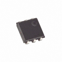
DS2417P+ Maxim Integrated Products, DS2417P+ Datasheet

DS2417P+
Specifications of DS2417P+
Related parts for DS2417P+
DS2417P+ Summary of contents
Page 1
... Time Chip with Interrupt PIN ASSIGNMENT PIN DESCRIPTION Pin 1 Pin 2 Pin 3 Pin 4 voltage range of Pin 5 Pin 6 ORDERING INFORMATION DS2417P DS2417P/T&R DS2417P+ DS2417P+T&R DS2417X + Denotes a lead(Pb)-free/RoHS-compliant package TSOC 150 mil 2 5 Top view ...
Page 2
OVERVIEW The DS2417 has two main data components: 1) 64-bit lasered ROM, and 2) real-time clock counter (Figure 1). The real-time clock utilizes an on-chip oscillator that is connected to an external 32.768kHz crystal. The hierarchical structure of the 1-Wire ...
Page 3
LASERED ROM Each DS2417 contains a unique ROM code that is 64 bits long. The first eight bits are a 1-Wire family code. The next 48 bits are a unique serial number. The last eight bits are a CRC ...
Page 4
CRC GENERATOR Figure 4 1ST 2ND 3RD STAGE STAGE STAGE TIMEKEEPING A 32.768kHz crystal oscillator is used as the time base for the real-time clock counter. The oscillator can be turned on ...
Page 5
IS Interval Select Bit These bits determine the time between interrupt pulses. The values available are shown below. IS2 IS1 IS0 32s 64s ...
Page 6
CLOCK FUNCTION COMMAND FLOW CHART Figure 5 Master TX Control Function Command 66H Read Clock ? Y DS2417 copies RTC Counter to R/W Buffer Bus Master RX Device Control Byte Bus Master RX LS Byte (7:0) Bus Master RX next ...
Page 7
HARDWARE CONFIGURATION Figure 6 BUS MASTER Open Drain Port Pin RX TX 1-WIRE BUS SYSTEM The 1-Wire bus is a system, which has a single bus master and one or more slaves. In all instances the DS2417 is a slave ...
Page 8
INITIALIZATION All transactions on the 1-Wire bus begin with an initialization sequence. The initialization sequence con- sists of a reset pulse transmitted by the bus master followed by presence pulse(s) transmitted by the slave(s). The presence pulse lets the bus ...
Page 9
ROM FUNCTIONS FLOW CHART Figure 7 33H N Read ROM Command ? Y DS2417 TX Family Code 1 Byte DS2417 TX Serial Number 6 Bytes DS2417 TX Master TX Bit 63 CRC Byte Master TX Reset Pulse DS2417 TX Presence ...
Page 10
SIGNALING The DS2417 requires strict protocols to ensure data integrity. The protocol consists of four types of sig- naling on one line: Reset Sequence with Reset Pulse and Presence Pulse, Write 0, Write 1, and Read Data. Except for ...
Page 11
READ/WRITE TIMING DIAGRAM Figure 9 Write-one Time Slot V PULLUP V PULLUP MIN V IH MIN V IL MAX 0V RESISTOR MASTER Write-zero Time Slot V PULLUP V PULLUP MIN V IH MIN V IL MAX 0V RESISTOR MASTER t ...
Page 12
READ/WRITE TIMING DIAGRAM (continued) Figure 9 Read-data Time Slot V PULLUP V PULLUP MIN V IH MIN V IL MAX 0V RESISTOR MASTER DS2417 CRYSTAL PLACEMENT ON PCB Figure 10 LOCAL GROUND PLANE BENEATH SIGNAL PLANE OR ON OTHER SIDE ...
Page 13
INTERRUPT TIMING Figure 11 V INT Case A: Latency < 0.5 t LATENCY V INT t LATENCY The latency depends on the selected interrupt interval (IS0 to IS2 settings) and the contents of the RTC counter at the time of ...
Page 14
ABSOLUTE MAXIMUM RATINGS* Voltage on 1-Wire to Ground Operating Temperature Range Storage Temperature Range Soldering Temperature * This is a stress rating only and functional operation of the device at these or any other conditions above those indicated in the ...
Page 15
NOTES: 1. All voltages are referenced to ground. 2. Measured with outputs open external pullup voltage. PUP 4. Input load is to ground. 5. Read data setup time refers to the time the host must pull the ...


