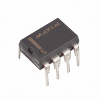
DS1672-33+ Maxim Integrated Products, DS1672-33+ Datasheet

DS1672-33+
Specifications of DS1672-33+
Related parts for DS1672-33+
DS1672-33+ Summary of contents
Page 1
... GENERAL DESCRIPTION The DS1672 incorporates a 32-bit counter and power-monitoring functions. The 32-bit counter is designed to count seconds and can be used to derive time-of-day, week, month, month, and year by using a software algorithm. A precision, temperature-compensated comparator circuit monitors the status of V When an out-of-tolerance condition occurs, an internal power-fail signal is generated that forces the reset to the active state ...
Page 2
... DS1672U-33 -40°C to +85°C DS1672U-33+ -40°C to +85°C DS1672U-33/T&R -40°C to +85°C DS1672U-33+T&R -40°C to +85°C + Denotes a lead(Pb)-free/RoHS-compliant device “+” anywhere on the top mark denotes a lead-free device 2-digit alphanumeric revision code. VOLTAGE (V) PIN-PACKAGE 2.0 8 DIP (300 mils) 3 ...
Page 3
... Leakage Current BACKUP Logic 0 Output (V = 0.4V > 2V; CC Logic 0.4V) OL Output (V < 2V; CC (DS1672- 0 Note 1: All voltages referenced to ground. Note 2: I specified with SCL clocking at max frequency (400kHz), trickle charger disabled. CCA Note 3: I specified with CCS CC CCTYP Note 4: SDA and RST. SYMBOL ...
Page 4
DC ELECTRICAL CHARACTERISTICS ( -40C to +85C PARAMETER V Current (Oscillator On) BACKUP V Current (Oscillator Off) BACKUP Note 5: Using the recommended crystal on X1 and X2. CRYSTAL SPECIFICATIONS PARAMETER Nominal Frequency Series ...
Page 5
AC ELECTRICAL CHARACTERISTICS ( -40C to +85C PARAMETER SYMBOL SCL Clock f SCL Frequency Bus Free Time Between a STOP and t BUF START Condition Hold Time (Repeated) START t HD:STA Condition LOW Period ...
Page 6
POWER-UP/POWER-DOWN CHARACTERISTICS (T = -40C to +85C) A PARAMETER V Detect to RST (V Falling Detect to RST (V Rising Fall Time PF(MAX) PF(MIN) V Rise Time ...
Page 7
... X1, X2 crystal layout considerations, refer to Application Note 58: Crystal Considerations with Dallas Real-Time Clocks. The DS1672 can also be driven by an external 32.768kHz oscillator. In this configuration, the X1 pin is connected to the external oscillator signal and the X2 pin is floated Battery Input for Any Standard 3V Lithium Cell or Other Energy Source. ...
Page 8
... SDA Oscillator Circuit The DS1672 uses an external 32.768kHz crystal. The oscillator circuit does not require any external resistors or capacitors to operate. Table 1 specifies several crystal parameters for the external crystal. Figure 4 shows a functional schematic of the oscillator circuit. If using a crystal with the specified characteristics, the startup time is usually less than one second. ...
Page 9
... Note 58: “Crystal Considerations with Dallas Real-Time Clocks” for detailed information. Address Map The counter is accessed by reading or writing the first 4 bytes of the DS1672 (00h–03h). The control register and trickle charger are accessed by reading or writing the appropriate register bytes as illustrated in Table 2. If the master continues to send or request more data after the address pointer has reached 05h, the address pointer will wrap around to location 00h ...
Page 10
... In order to prevent accidental enabling, only a pattern on 1010 will enable the trickle charger. All other patterns will disable the trickle charger. The DS1672 powers up with the trickle charger disabled. The diode select (DS) bits (bits 2, 3) select whether or not a diode is ...
Page 11
Figure 5. Programmable Trickle Charger SELECT NOTE: ONLY 1010 ENABLES TCS TCS TCS TCS BIT 7 BIT 6 BIT 5 BIT 4 TRICKLE CHARGE REGISTER SELECT SELECT DS DS ...
Page 12
... START and STOP conditions. The DS1672 operates as a slave on the I are made via the open-drain I/O lines SDA and SCL. Within the bus specifications, a standard mode (100kHz maximum clock rate) and a fast mode (400kHz maximum clock rate) are defined. The DS1672 operates in both modes. ...
Page 13
... The master will generate a stop condition to terminate the data write. 2) Slave transmitter mode (DS1672 read mode): The first byte is received and handled as in the slave receiver mode. However, in this mode, the direction bit will indicate that the transfer direction is reversed ...
Page 14
Figure 6. Data Transfer on I SDA MSB SCL 1 START CONDITION Figure 7. Data Write: Slave Receiver Mode <Slave Address> <Word Address (n)> S 1101000 0 A XXXXXXXX S - START A - ACKNOW LEDGE P - STOP R/W ...
Page 15
... No circuit patent licenses are implied. Maxim/Dallas Semiconductor reserves the right to change the circuitry and specifications without notice at any time The Maxim logo is a registered trademark of Maxim Integrated Products, Inc. The Dallas logo is a registered trademark of Dallas Semiconductor Corporation. THETA-JC 40°C/W 40°C/W 39°C/W DOCUMENT NO. 21-0043 21-0041 21-0036 © 2006 Maxim Integrated Products DS1672 ...


