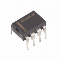
DS1307+ Maxim Integrated Products, DS1307+ Datasheet - Page 12

DS1307+
Manufacturer Part Number
DS1307+
Description
IC RTC SERIAL 512K 8-DIP
Manufacturer
Maxim Integrated Products
Type
Clock/Calendar/NVSRAMr
Datasheet
1.DS1307Z.pdf
(14 pages)
Specifications of DS1307+
Memory Size
56B
Time Format
HH:MM:SS (12/24 hr)
Date Format
YY-MM-DD-dd
Interface
I²C, 2-Wire Serial
Voltage - Supply
4.5 V ~ 5.5 V
Operating Temperature
0°C ~ 70°C
Mounting Type
Through Hole
Package / Case
8-DIP (0.300", 7.62mm)
Function
Clock/Calendar
Rtc Memory Size
56 Byte
Supply Voltage (max)
5.5 V
Supply Voltage (min)
4.5 V
Maximum Operating Temperature
+ 70 C
Minimum Operating Temperature
0 C
Mounting Style
Through Hole
Rtc Bus Interface
Serial (I2C)
Supply Current
1.5 mA
Lead Free Status / RoHS Status
Lead free / RoHS Compliant
The DS1307 can operate in the following two modes:
Figure 4. Data Write—Slave Receiver Mode
Figure 5. Data Read—Slave Transmitter Mode
S - Start
A - Acknowledge (ACK)
P - Stop
S - Start
A - Acknowledge (ACK)
P - Stop
A - Not Acknowledge (NACK)
S
S
<Slave Address>
<Slave Address>
1101000
1101000
1. Slave Receiver Mode (Write Mode): Serial data and clock are received through SDA and SCL. After
2. Slave Transmitter Mode (Read Mode): The first byte is received and handled as in the slave receiver
each byte is received an acknowledge bit is transmitted. START and STOP conditions are recognized
as the beginning and end of a serial transfer. Hardware performs address recognition after reception of
the slave address and direction bit (see Figure 4). The slave address byte is the first byte received
after the master generates the START condition. The slave address byte contains the 7-bit DS1307
address, which is 1101000, followed by the direction bit (R/W), which for a write is 0. After receiving and
decoding the slave address byte, the DS1307 outputs an acknowledge on SDA. After the DS1307
acknowledges the slave address + write bit, the master transmits a word address to the DS1307. This
sets the register pointer on the DS1307, with the DS1307 acknowledging the transfer. The master can
then transmit zero or more bytes of data with the DS1307 acknowledging each byte received. The
register pointer automatically increments after each data byte are written. The master will generate a
STOP condition to terminate the data write.
mode. However, in this mode, the direction bit will indicate that the transfer direction is reversed. The
DS1307 transmits serial data on SDA while the serial clock is input on SCL. START and STOP
conditions are recognized as the beginning and end of a serial transfer (see Figure 5). The slave
address byte is the first byte received after the START condition is generated by the master. The slave
address byte contains the 7-bit DS1307 address, which is 1101000, followed by the direction bit (R/W),
which is 1 for a read. After receiving and decoding the slave address the DS1307 outputs an
acknowledge on SDA. The DS1307 then begins to transmit data starting with the register address
pointed to by the register pointer. If the register pointer is not written to before the initiation of a read
mode the first address that is read is the last one stored in the register pointer. The register pointer
automatically increments after each byte are read. The DS1307 must receive a Not Acknowledge to
end a read.
0
1
A
A
<Word Address (n)>
XXXXXXXX
XXXXXXXX
<Data(n)>
Slave to master
Master to slave
Slave to master
Master to slave
A
A
XXXXXXXX
XXXXXXXX
<Data(n+1)>
<Data(n)>
(X+1 BYTES + ACKNOWLEDGE); NOTE: LAST DATA BYTE IS
FOLLOWED BY A NOT ACKNOWLEDGE (A) SIGNAL)
(X+1 BYTES + ACKNOWLEDGE)
A XXXXXXXX
A XXXXXXXX
<Data(n+2)>
DATA TRANSFERRED
<Data(n+1)>
DATA TRANSFERRED
12 of 14
A
A
<Data(n+X)>
...
...
XXXXXXXX
XXXXXXXX
<Data(n+X)>
DS1307 64 x 8, Serial, I
A P
A P
2
C Real-Time Clock


