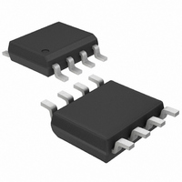
DS1388Z-5+ Maxim Integrated Products, DS1388Z-5+ Datasheet - Page 12

DS1388Z-5+
Manufacturer Part Number
DS1388Z-5+
Description
IC RTC I2C W/CHARGER 8-SOIC
Manufacturer
Maxim Integrated Products
Type
Clock/Calendar/Supervisor/EEPROMr
Datasheet
1.DS1388Z-33.pdf
(19 pages)
Specifications of DS1388Z-5+
Memory Size
4K (512 x 8)
Time Format
HH:MM:SS:hh (12/24 hr)
Date Format
YY-MM-DD-dd
Interface
I²C, 2-Wire Serial
Voltage - Supply
4.5 V ~ 5.5 V
Operating Temperature
-40°C ~ 85°C
Mounting Type
Surface Mount
Package / Case
8-SOIC (3.9mm Width)
Lead Free Status / RoHS Status
Lead free / RoHS Compliant
The contents of the watchdog alarm counter, which is a
separate two-byte BCD down counter, are accessed in
the address range 08h–09h in block 0h. It is programma-
ble in 10ms intervals from 0.01 to 99.99 seconds. When
this counter is written, both the counter and a seed regis-
ter are loaded with the desired value. When the counter is
to be reloaded, it uses the value in the seed register.
When the counter is read, the current counter value is
latched into a register, which is output on the serial data
line and the watchdog counter reloads the seed value.
If the counter is not needed, it can be disabled and
used as a 16-bit cache of battery-backed RAM by set-
ting the WDE bit in the control register to logic 0. If all
16 bits of the watchdog alarm counter are written to a
zero when WDE = 1, the counter is disabled and the
WF bit is not set.
When the WDE bit in the control register is set to a logic
1 and a non-zero value is written into the watchdog reg-
isters, the watchdog alarm counter decrements every
1/100 second, until it reaches zero. At this point, the WF
bit in the flag register is set. If WD/RST = 1, the RST pin
is pulsed low for t
inhibited. At the end of t
impedance, and read/write access to the DS1388 is
enabled. The WF flag remains set until cleared by writ-
ing WF to logic 0. The watchdog alarm counter can be
reloaded and restarted before the counter reaches zero
by reading or writing any of the watchdog alarm
counter registers.
The WF flag and WDE bit must be set to zero before writing
the watchdog registers. After writing the watchdog regis-
ters, WDE must be set to one to enable the watchdog.
A precision temperature-compensated reference and
comparator circuit monitors the status of V
out-of-tolerance condition occurs, an internal power-fail
signal is generated that blocks read/write access to the
device and forces the RST pin low. When V
to an in-tolerance condition, the internal power-fail sig-
nal is held active for t
stabilize, and the RST pin is held low. If the EOSC bit is
set to a logic 1 (to disable the oscillator in battery-back-
up mode), the internal power-fail signal and the RST pin
are kept active for t
I
and 512 Bytes EEPROM
12
2
C RTC/Supervisor with Trickle Charger
BIT 7
OSF
____________________________________________________________________
Pushbutton Reset Functions
Power-Up/Down, Reset, and
Watchdog Alarm Counter
RST
BIT 6
RST
WF
RST
plus the oscillator startup time.
RST
and access to the DS1388 is
to allow the power supply to
, the RST pin becomes high
BIT 5
0
CC
CC
. When an
BIT 4
returns
0
Access is inhibited whenever RST is low.
The DS1388 provides for a pushbutton switch to be
connected to the RST output pin. When the DS1388 is
not in a reset cycle, it continuously monitors the RST
signal for a low-going edge. If an edge is detected, the
part debounces the switch by pulling the RST pin low
and inhibits read/write access. After the internal timer
has expired, the part continues to monitor the RST line.
If the line is still low, it continues to monitor the line look-
ing for a rising edge. Upon detecting release, the part
forces the RST pin low and holds it low for t
The DS1388 has three additional registers (control,
flag, and trickle charger) that control the real-time
clock, watchdog, and trickle charger.
Bit 7: Oscillator Stop Flag (OSF). A logic 1 in this bit
indicates that the oscillator has stopped or was
stopped for some period of time and may be used to
judge the validity of the clock and calendar data. This
bit is edge triggered and is set to logic 1 when the
internal circuitry senses the oscillator has transitioned
from a normal run state to a STOP condition. The follow-
ing are examples of conditions that can cause the OSF
bit to be set:
1) The first time power is applied.
2) The voltage present on both V
3) The EOSC bit is turned off.
4) External influences on the crystal (i.e., noise, leak-
This bit remains at logic 1 until written to logic 0. This
bit can only be written to logic 0. Attempting to write
OSF to logic 1 leaves the value unchanged.
Bit 6: Watchdog Alarm Flag (WF). A logic 1 in this bit
indicates that the watchdog counter reached zero. If
WDE and WD/RST are set to 1, the RST pin pulses low
for t
sets WF = 1. At the completion of the pulse, the WF bit
remains set to logic 1. Writing this bit to logic 0 clears
the WF flag. This bit can only be written to logic 0.
Attempting to write logic 1 leaves the value unchanged.
Bits 5 to 0: These bits read as zero and cannot be
modified.
BIT 3
insufficient to support oscillation.
age, etc.).
RST
0
when the watchdog counter reaches zero and
Special-Purpose Registers
BIT 2
0
Flag Register (00Bh)
Flag Register (00Bh)
BIT 1
0
CC
and V
RST
BACKUP
BIT 0
.
0
are


