DS1388Z-3+ Maxim Integrated Products, DS1388Z-3+ Datasheet - Page 10

DS1388Z-3+
Manufacturer Part Number
DS1388Z-3+
Description
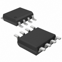
IC RTC I2C W/CHARGER 8-SOIC
Manufacturer
Maxim Integrated Products
Type
Clock/Calendar/Supervisor/EEPROMr
Datasheet
1.DS1388Z-33.pdf
(19 pages)
Specifications of DS1388Z-3+
Memory Size
4K (512 x 8)
Time Format
HH:MM:SS:hh (12/24 hr)
Date Format
YY-MM-DD-dd
Interface
I²C, 2-Wire Serial
Voltage - Supply
2.7 V ~ 3.3 V
Operating Temperature
-40°C ~ 85°C
Mounting Type
Surface Mount
Package / Case
8-SOIC (3.9mm Width)
Lead Free Status / RoHS Status
Lead free / RoHS Compliant
I
and 512 Bytes EEPROM
The accuracy of the clock is dependent upon the accu-
racy of the crystal and the accuracy of the match
between the capacitive load of the oscillator circuit and
the capacitive load for which the crystal was trimmed.
Additional error is added by crystal frequency drift
caused by temperature shifts. External circuit noise
coupled into the oscillator circuit can result in the clock
running fast. Figure 3 shows a typical PC board layout
for isolation of the crystal and oscillator from noise.
Refer to Application Note 58: Crystal Considerations
with Dallas Real-Time Clock s for detailed information.
Figure 4 shows the address map for the DS1388. The
memory map is divided into three blocks. The memory
block accessed is determined by the value of the block
address bits in the slave address byte. The timekeep-
ing registers reside in block 0h. During a multibyte
access of the timekeeping registers, when the internal
address pointer reaches 0Ch, it wraps around to loca-
tion 00h. On an I
menting to location 00h, the current time is transferred
to a second set of registers. The time information is
read from these secondary registers, while the clock
may continue to run. This eliminates the need to reread
the registers in case the main registers update during a
Figure 3. Layout Example
10
2
C RTC/Supervisor with Trickle Charger
____________________________________________________________________
2
C START or address pointer incre-
LOCAL GROUND PLANE (LAYER 2)
NOTE: AVOID ROUTING SIGNAL LINES
IN THE CROSSHATCHED AREA
(UPPER LEFT QUADRANT) OF
THE PACKAGE UNLESS THERE IS
A GROUND PLANE BETWEEN THE
SIGNAL LINE AND THE DEVICE PACKAGE.
Clock Accuracy
Address Map
CRYSTAL
read. The EEPROM is divided into two 256-byte blocks
located in blocks 1h and 2h. During a multibyte read of
the EEPROM registers, when the internal address point-
er reaches FFh, it wraps around to location 00h of the
block of EEPROM specified in the block address.
During a multibyte write of the EEPROM registers, when
the internal address pointer reaches the end of the cur-
rent 8-byte EEPROM page, it wraps around to the
beginning of the EEPROM page. See the Write
Operation section for details.
To avoid rollover issues when writing to the time and
date registers, all registers should be written before the
hundredths-of-seconds register reaches 99 (BCD).
The hundredths-of-seconds generator circuit shown in
the Block Diagram is a state machine that divides the
incoming frequency (4096Hz) by 41 for 24 cycles and
40 for 1 cycle. This produces a 100Hz output that is
slightly off during the short term, and is exactly correct
every 250ms. The divide ratio is given by:
Thus, the long-term average frequency output is
exactly 100Hz.
GND
X1
X2
Ratio = [41 x 24 + 40 x 1] / 25 = 40.96
Hundredths-of-Seconds
Generator


