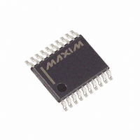
DS1306E+ Maxim Integrated Products, DS1306E+ Datasheet

DS1306E+
Specifications of DS1306E+
Related parts for DS1306E+
DS1306E+ Summary of contents
Page 1
Rev 12/09 www.maxim-ic.com FEATURES Real-Time Clock (RTC) Counts Seconds, Minutes, Hours, Date of the Month, Month, Day of the Week, and Year with Leap-Year Compensation Valid Up to 2100 96-Byte, Battery-Backed NV RAM for Data Storage ...
Page 2
... ORDERING INFORMATION PART DS1306 DS1306+ DS1306N DS1306N+ DS1306E DS1306E+ DS1306EN DS1306EN+ DS1306EN/T&R DS1306EN+T&R DS1306E/T&R DS1306E+T&R +Denotes a lead(Pb)-free/RoHS-compliant package T&R = Tape and reel. *An “N” on the top mark indicates an industrial device. PIN DESCRIPTION PIN NAME TSSOP DIP CC2 BAT INT0 8 6 INT1 ...
Page 3
PIN DESCRIPTION (continued) PIN NAME TSSOP DIP 9 7 1Hz 10 8 GND 11 9 SERMODE SCLK 15 12 SDI 16 13 SDO CCIF 18 15 32kHz CC1 4, ...
Page 4
DESCRIPTION The DS1306 serial alarm real-time clock (RTC) provides a full binary coded decimal (BCD) clock calendar that is accessed by a simple serial interface. The clock/calendar provides seconds, minutes, hours, day, date, month, and year information. The end of ...
Page 5
RECOMMENDED LAYOUT FOR CRYSTAL Local ground plane (Layer 2) crystal CLOCK ACCURACY The accuracy of the clock is dependent upon the accuracy of the crystal and the accuracy of the match between the capacitive load of the oscillator circuit and ...
Page 6
Figure 2. RTC REGISTERS AND ADDRESS MAP HEX ADDRESS Bit7 Bit6 READ WRITE 00h 80h 0 01h 81h 0 02h 82h 0 03h 83h 0 04h 84h 0 05h 85h 0 06h 86h 07h 87h M 08h 88h M 09h ...
Page 7
Similarly, an alarm is generated every minute when bit 7 of the day, hour, and minute alarm registers is set to a logic 1. When bit 7 of the day, hour, minute, and ...
Page 8
STATUS REGISTER (READ 10H) BIT7 BIT6 0 0 IRQF0 (Interrupt 0 Request Flag) – A logic 1 in the interrupt request flag bit indicates that the current time has matched the Alarm 0 registers. If the AIE0 bit is also ...
Page 9
Table 3. TRICKLE CHARGER RESISTOR AND DIODE SELECT TCS TCS TCS TCS Bit 7 Bit 6 Bit 5 Bit ...
Page 10
Figure 4. POWER-SUPPLY CONFIGURATIONS NOTE: DEVICE IS WRITE-PROTECTED IF V NOTE: DEVICE DOES NOT PROVIDE AUTOMATIC WRITE PROTECTION. CONFIGURATION 1: BACKUP SUPPLY IS NONRECHARGEABLE LITHIUM BATTERY < CCTP CONFIGURATION 2: BACKUP SUPPLY IS A RECHARGEABLE BATTERY OR ...
Page 11
SERIAL INTERFACE The DS1306 offers the flexibility to choose between two serial interface modes. The DS1306 can communicate with the SPI interface or with a standard 3-wire interface. The interface method used is determined by the SERMODE pin. When this ...
Page 12
ADDRESS AND DATA BYTES Address and data bytes are shifted MSB first into the serial data input (SDI) and out of the serial data output (SDO). Any transfer requires the address of the byte to specify a write or read ...
Page 13
Figure 8. SPI MULTIPLE-BYTE BURST TRANSFER READING AND WRITING IN BURST MODE Burst mode is similar to a single-byte read or write, except that CE is kept high and additional SCLK cycles are sent until the end of the burst. ...
Page 14
Figure 9. 3-WIRE SINGLE BYTE TRANSFER CE SCLK I/ SCLK I/ NOTE: IN BURST MODE KEPT HIGH AND ADDITIONAL SCLK CYCLES ARE SENT UNTIL THE END OF THE BURST. *I/O IS SDI ...
Page 15
ABSOLUTE MAXIMUM RATINGS Voltage Range on Any Pin Relative to Ground……………………………………………..-0.5V to +7.0V Storage Temperature Range……………………………………………………………….-55C to +125C Soldering Temperature.……………………………….Refer to the IPC/JEDEC Standard J-STD-020 This is a stress rating only and functional operation of the device at these or ...
Page 16
DC ELECTRICAL CHARACTERISTICS (T = Over the operating range, unless otherwise specified.) A PARAMETER Input Leakage Output Leakage I = 1.5mA OL Logic 0 Output I = 4.0mA -0.4mA OH Logic 1 Output I = -1.0mA OH ...
Page 17
AC ELECTRICAL CHARACTERISTICS (T = Over the operating range, unless otherwise specified.) (Figure 10 and Figure 11) A PARAMETER Data to CLK Setup CLK to Data Hold CLK to Data Delay CLK Low Time CLK High Time CLK Frequency ...
Page 18
Figure 10. TIMING DIAGRAM: 3-WIRE READ DATA TRANSFER SERMODE = GND * I/O IS SDI AND SDO TIED TOGETHER. Figure 11. TIMING DIAGRAM: 3-WIRE WRITE DATA TRANSFER SERMODE = GND * I/O IS SDI AND SDO TIED TOGETHER ...
Page 19
SPI AC ELECTRICAL CHARACTERISTICS (T = Over the operating range, unless otherwise specified.) A PARAMETER Data to CLK Setup CLK to Data Hold CLK to Data Delay CLK Low Time CLK High Time CLK Frequency CLK Rise and Fall CE ...
Page 20
Figure 12. TIMING DIAGRAM: SPI READ DATA TRANSFER SERMODE = SCLK CAN BE EITHER POLARITY, TIMING SHOWN FOR CPOL = 1. Figure 13. TIMING DIAGRAM: SPI WRITE DATA TRANSFER SERMODE = SCLK CAN BE ...
Page 21
NOTES and I are specified with CE set to a logic 0. CC1T CC2T 2) I and I are specified with CC1A CC2A 2.0V 0V Measured ...
Page 22
... Maxim cannot assume responsibility for use of any circuitry other than circuitry entirely embodied in a Maxim product. No circuit patent licenses are implied. Maxim reserves the right to change the circuitry and specifications without notice at any time © 2009 Maxim Integrated Products DESCRIPTION ” to Figures 6, 7, 12, and 13 Maxim Is a registered trademark of Maxim Integrated Products, Inc. DS1306 PAGES CHANGED 5 12 ...


