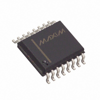
DS3231S# Maxim Integrated Products, DS3231S# Datasheet - Page 13

DS3231S#
Manufacturer Part Number
DS3231S#
Description
IC RTC W/TCXO 16-SOIC
Manufacturer
Maxim Integrated Products
Type
Clock/Calendar/TCXO/Crystalr
Datasheet
1.DS3231S.pdf
(20 pages)
Specifications of DS3231S#
Time Format
HH:MM:SS (12/24 hr)
Date Format
YY-MM-DD-dd
Interface
I²C, 2-Wire Serial
Voltage - Supply
2.3 V ~ 5.5 V
Operating Temperature
0°C ~ 70°C
Mounting Type
Surface Mount
Package / Case
16-SOIC (0.300", 7.5mm Width)
Function
Clock/Calendar/Battery Backup
Supply Voltage (max)
5.5 V
Supply Voltage (min)
2.3 V
Maximum Operating Temperature
+ 70 C
Minimum Operating Temperature
0 C
Mounting Style
SMD/SMT
Rtc Bus Interface
Serial (I2C)
Lead Free Status / RoHS Status
Lead free / RoHS Compliant
Memory Size
-
Lead Free Status / Rohs Status
Lead free / RoHS Compliant
Available stocks
Company
Part Number
Manufacturer
Quantity
Price
The DS3231 has two additional registers (control and
status) that control the real-time clock, alarms, and
square-wave output.
Bit 7: Enable Oscillator (EOSC). When set to logic 0,
the oscillator is started. When set to logic 1, the oscilla-
tor is stopped when the DS3231 switches to V
bit is clear (logic 0) when power is first applied. When
the DS3231 is powered by V
on regardless of the status of the EOSC bit. When
EOSC is disabled, all register data is static.
Bit 6: Battery-Backed Square-Wave Enable
(BBSQW). When set to logic 1 with INTCN = 0 and V
< V
is logic 0, the INT/SQW pin goes high impedance when
V
first applied.
Bit 5: Convert Temperature (CONV). Setting this bit to
1 forces the temperature sensor to convert the temper-
ature into digital code and execute the TCXO algorithm
to update the capacitance array to the oscillator. This
can only happen when a conversion is not already in
progress. The user should check the status bit BSY
before forcing the controller to start a new TCXO exe-
cution. A user-initiated temperature conversion does
not affect the internal 64-second update cycle.
A user-initiated temperature conversion does not affect
the BSY bit for approximately 2ms. The CONV bit
remains at a 1 from the time it is written until the conver-
sion is finished, at which time both CONV and BSY go
to 0. The CONV bit should be used when monitoring
the status of a user-initiated conversion.
Bits 4 and 3: Rate Select (RS2 and RS1). These bits
control the frequency of the square-wave output when
the square wave has been enabled. The following table
CC
NAME:
PF
POR:
< V
, this bit enables the square wave. When BBSQW
PF
. This bit is disabled (logic 0) when power is
Special-Purpose Registers
BIT 7
0
Control Register (0Eh)
BBSQW
CC
BIT 6
Extremely Accurate I
, the oscillator is always
0
____________________________________________________________________
CONV
BIT 5
0
BAT
. This
CC
BIT 4
RS2
1
shows the square-wave frequencies that can be select-
ed with the RS bits. These bits are both set to logic 1
(8.192kHz) when power is first applied.
Bit 2: Interrupt Control (INTCN). This bit controls the
INT/SQW signal. When the INTCN bit is set to logic 0, a
square wave is output on the INT/SQW pin. When the
INTCN bit is set to logic 1, then a match between the
timekeeping registers and either of the alarm registers
activates the INT/SQW output (if the alarm is also
enabled). The corresponding alarm flag is always set
regardless of the state of the INTCN bit. The INTCN bit
is set to logic 1 when power is first applied.
Bit 1: Alarm 2 Interrupt Enable (A2IE). When set to
logic 1, this bit permits the alarm 2 flag (A2F) bit in the
status register to assert INT/SQW (when INTCN = 1).
When the A2IE bit is set to logic 0 or INTCN is set to
logic 0, the A2F bit does not initiate an interrupt signal.
The A2IE bit is disabled (logic 0) when power is first
applied.
Bit 0: Alarm 1 Interrupt Enable (A1IE). When set to
logic 1, this bit permits the alarm 1 flag (A1F) bit in the
status register to assert INT/SQW (when INTCN = 1).
When the A1IE bit is set to logic 0 or INTCN is set to
logic 0, the A1F bit does not initiate the INT/SQW sig-
nal. The A1IE bit is disabled (logic 0) when power is
first applied.
SQUARE-WAVE OUTPUT FREQUENCY
RS2
0
0
1
1
BIT 3
RS1
1
RTC/TCXO/Crystal
RS1
0
1
0
1
INTCN
BIT 2
2
1
C-Integrated
Control Register (0Eh)
SQUARE-WAVE OUTPUT
FREQUENCY
BIT 1
A2IE
1.024kHz
4.096kHz
8.192kHz
0
1Hz
BIT 0
A1IE
0
13


