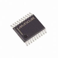
DS1670E+ Maxim Integrated Products, DS1670E+ Datasheet

DS1670E+
Specifications of DS1670E+
Related parts for DS1670E+
DS1670E+ Summary of contents
Page 1
... PACKAGE DS1670E 3.3 20 TSSOP DS1670E+ 3.3 20 TSSOP DS1670E/T&R 3.3 20 TSSOP DS1670E+TRL 3.3 20 TSSOP DS1670S 3 DS1670S+ 3 All devices are specified over the 0°C to +70°C operating range. † A “‘+” anywhere on the top mark denotes a lead-free device. + Denotes a lead(Pb)-free/RoHS-compliant device. ...
Page 2
DETAILED DESCRIPTION The microprocessor monitor circuitry of the DS1670 provides three basic functions. First, a precision temperature-compensated reference and comparator circuit monitors the status of V tolerance condition occurs, an internal power-fail signal is generated that forces the reset to ...
Page 3
PIN DESCRIPTION PIN NAME Battery Input for Standard 3V Lithium Cell or Other Energy Source. UL recognized ensure against reverse charging when used with a lithium battery BAT ic.com/qa/info/ul/. External SRAM Power Supply Output. This ...
Page 4
POWER-UP/POWER-DOWN CONSIDERATIONS The DS1670 was designed to operate with a power supply of 3.3V. When 3.3V are applied within nominal limits, the device becomes fully accessible after t inputs are disabled. When V CC below the lower of 2.7V (typical) ...
Page 5
CLOCK, CALENDAR, AND ALARM The time and calendar information is accessed by reading/writing the appropriate register bytes. Note that some bits are set to 0. These bits will always read 0 regardless of how they are written. Also note that ...
Page 6
AIS0-AIS1 (Analog Input Select). These 2 bits are used to determine the analog input for the analog-to- digital conversion. Table 2 lists the specific analog input that is selected by these two bits. AIE (Alarm Interrupt Enable). When set to ...
Page 7
The DS1670 nonvolatilizes the external SRAM(s) by write protecting the SRAM(s) and by providing a back-up power supply in the absence of V external SRAM(s) are prohibited by forcing and . Also at this point, the SRAM power supply (V ...
Page 8
After the internal 250ms timer has expired, the DS1670 will continue RST to monitor the line. If the line is still low, the DS1670 will continue to monitor the line looking for a RST ...
Page 9
Note also that the converter can be turned off by these bits to reduce power. When the ADC is turned on by setting AIS0 and AIS1 to any value other than 0,0 ...
Page 10
Address and data bytes are always shifted LSB first into the I/O pin. Any transaction requires the address/command byte to specify a read or write to a specific register followed by one or more bytes of data. The address byte ...
Page 11
ABSOLUTE MAXIMUM RATINGS Voltage on Any Pin Relative to Ground………………………………………………………-0.3V to +6V Operating Temperature………………………………………………………………………..0°C to +70°C Storage Temperature………………………………………………………………………-55°C to +125°C Soldering Temperature………………………………………….See IPC/JEDEC J-STD-020 Specification This is a stress rating only and functional operation of the device at these or ...
Page 12
DC ELECTRICAL CHARACTERISTICS PARAMETER Input Leakage CS Leakage Logic 1 Output (I =-0.4 mA) out Logic 0 Output (I =1.5 mA) out Active Supply Current ( -0.2) CC A/D Converter Current Standby Current (CS Battery Current ...
Page 13
AC ELECTRICAL CHARACTERISTICS PARAMETER Data to Clock Setup CLK to Data Hold CLK to Data Delay CLK to Low Time CLK to High Time CLK Frequency CLK Rise and Fall CS to CLK Setup CLK to CS Hold CS Inactive ...
Page 14
TIMING DIAGRAM: READ DATA Figure 9 TIMING DIAGERAM: WRITE DATA Figure DS1670 ...
Page 15
PUSHBUTTON RESET Figure 11 RST POWER-UP Figure RST POWER-DOWN Figure RST CCTP t RPU CCTPMAX V CCTP V CCSWMIN RPD t ...
Page 16
... Maxim/Dallas Semiconductor cannot assume responsibility for use of any circuitry other than circuitry entirely embodied in a Maxim/Dallas Semiconductor product. No circuit patent licenses are implied. Maxim/Dallas Semiconductor reserves the right to change the circuitry and specifications without notice at any time The Maxim logo is a registered trademark of Maxim Integrated Products, Inc. The Dallas logo is a registered trademark of Dallas Semiconductor Corporation. = 3.3V ...


