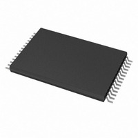
DS17885E-3+ Maxim Integrated Products, DS17885E-3+ Datasheet - Page 25

DS17885E-3+
Manufacturer Part Number
DS17885E-3+
Description
IC RTC 3V 8K NV RAM 28-TSOP
Manufacturer
Maxim Integrated Products
Type
Clock/Calendar/NVSRAMr
Datasheet
1.DS17285S-5.pdf
(31 pages)
Specifications of DS17885E-3+
Memory Size
64K (8K x 8)
Time Format
HH:MM:SS (12/24 hr)
Date Format
YY-MM-DD-dd
Interface
Parallel
Voltage - Supply
2.7 V ~ 3.7 V
Operating Temperature
0°C ~ 70°C
Mounting Type
Surface Mount
Package / Case
28-TSOP
Lead Free Status / RoHS Status
Lead free / RoHS Compliant
Two extended control registers are provided to supply
control and status information for the extended func-
tions offered by the DS17x85/DS17x87. These are des-
Bit 7: Valid RAM and Time 2 (VRT2). This status bit
gives the condition of the auxiliary battery. It is set to
logic 1 condition when the external lithium battery is
connected to the V
the external battery should be replaced.
Bit 6: Increment in Progress Status (INCR). This bit is
set to 1 when an increment to the time/date registers is
in progress and the alarm checks are being made.
INCR is set to 1 at 122µs before the update cycle starts
and is cleared to 0 at the end of each update cycle.
Bit 5: Burst Mode Enable (BME). The burst mode
enable bit allows the extended user RAM address reg-
isters to automatically increment for consecutive reads
and writes. When BME is set to logic 1, the automatic
incrementing is enabled and when BME is set to a logic
0, the automatic incrementing is disabled.
Figure 7. Burst Mode Timing Waveform
Extended Control Register (4Ah)
MSB
* Reserved bit. This bit is reserved for future use. It can be read and written, but has no effect on operation.
DS OR R/W
BIT 7
VRT2
AD0-7
CS
AS
Extended Control Registers
BIT 6
INCR
BAUX
. If this bit is read as logic 0,
53H
BIT 5
BME
____________________________________________________________________
BIT 4
*
PW
RWL
DATA
ignated as Extended Control Registers 4A and 4B, and
are located in register bank 1, locations 04AH and
04BH, respectively. The functions of the bits within
these registers are described as follows.
Bit 3: Power Active-Bar Control (PAB). When this bit
is 0, the PWR pin is in the active low state. When this bit
is 1, the PWR pin is in the high-impedance state. The
user can write this bit to logic 1 or 0. If either WF and
WIE = 1 or KF and KSE = 1, the PAB bit is cleared to 0.
Bit 2: RAM Clear Flag (RF). This bit is set to logic 1
when a high-to-low transition occurs on the RCLR input
if RCE = 1. Writing this bit to logic 0 clears it. This bit
can also be written to logic 1 to force an interrupt con-
dition.
Bit 1: Wake-Up Alarm Flag (WF). This bit is set to 1
when a wake-up alarm condition occurs or when the
user writes it to 1. WF is cleared by writing it to 0.
Bit 0: Kickstart Flag (KF). This bit is set to 1 when a
kickstart condition occurs or when the user writes it to
1. This bit is cleared by writing it to logic 0.
ADDRESS + 1
BIT 3
PAB
PW
RWH
Real-Time Clocks
BIT 2
RF
DATA
BIT 1
WF
ADDRESS + 2
BIT 0
KF
LSB
25


