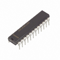
DS17887-5+ Maxim Integrated Products, DS17887-5+ Datasheet - Page 26

DS17887-5+
Manufacturer Part Number
DS17887-5+
Description
IC RTC 5V 8K NV RAM 24-EDIP
Manufacturer
Maxim Integrated Products
Type
Clock/Calendar/NVSRAMr
Datasheet
1.DS17285S-5.pdf
(31 pages)
Specifications of DS17887-5+
Memory Size
64K (8K x 8)
Time Format
HH:MM:SS (12/24 hr)
Date Format
YY-MM-DD-dd
Interface
Parallel
Voltage - Supply
4.5 V ~ 5.5 V
Operating Temperature
0°C ~ 70°C
Mounting Type
Through Hole
Package / Case
24-DIP (600 mil) Module
Function
Clock/Calendar/Alarm
Rtc Memory Size
8192 Byte
Supply Voltage (max)
5.5 V
Supply Voltage (min)
4.5 V
Maximum Operating Temperature
+ 70 C
Minimum Operating Temperature
0 C
Mounting Style
Through Hole
Rtc Bus Interface
Multiplexed
Supply Current
25 mA
Lead Free Status / RoHS Status
Lead free / RoHS Compliant
Real-Time Clocks
Bit 7: Auxiliary Battery Enable (ABE). When written to
logic 1, this bit enables the V
functions.
Bit 6: Enable 32.768kHz Output (E32k). When written
to logic 1, this bit enables the 32.768kHz oscillator fre-
quency to be output on the SQW pin. E32k is set to 1
when V
Bit 5: Crystal Select (CS). When CS is set to 0, the
oscillator is configured for operation with a crystal that
has a 6pF specified load capacitance. When CS = 1,
the oscillator is configured for a 12.5pF crystal. CS is
disabled in the DS17x87 module and should be set to
CS = 0.
Bit 4: RAM Clear Enable (RCE). When set to 1, this bit
enables a low level on RCLR to clear all 114 bytes of
user RAM. When RCE = 0, RCLR and the RAM clear
function are disabled.
Bit 3: PAB Reset Select (PRS). When set to 0, the
PWR pin is set high impedance when the DS17x85
goes into power fail. When set to 1, the PWR pin
remains active upon entering power fail.
Extended Control Register (4Bh)
MSB
26
BIT 7
ABE
____________________________________________________________________
CC
is powered up.
BIT 6
E32k
BAUX
BIT 5
CS
pin for extended
BIT 4
RCE
Bit 2: RAM Clear Interrupt Enable (RIE). When RIE is
set to 1, the IRQ pin is driven low when a RAM clear
function is completed.
Bit 1: Wake-Up Alarm Interrupt Enable (WIE). When
V
is driven active low when a wake-up condition occurs,
causing the WF bit to be set to 1. When V
applied, the IRQ pin is also driven low. If WIE is set
while system power is applied, both IRQ and PWR are
driven low in response to WF being set to 1. When WIE
is cleared to 0, the WF bit has no effect on the PWR or
IRQ pins.
Bit 0: Kickstart Interrupt Enable (KSE). When V
voltage is absent and KSE is set to 1, the PWR pin is
driven active low when a kickstart condition occurs (KS
pulsed low), causing the KF bit to be set to 1. When
V
KSE is set to 1 while system power is applied, both IRQ
and PWR are driven low in response to KF being set to
1. When KSE is cleared to 0, the KF bit has no effect on
the PWR or IRQ pins.
CC
CC
BIT 3
PRS
voltage is absent and WIE is set to 1, the PWR pin
is then applied, the IRQ pin is also driven low. If
BIT 2
RIE
BIT 1
WIE
CC
BIT 0
KSE
is then
LSB
CC


