DS1644P-120+ Maxim Integrated Products, DS1644P-120+ Datasheet
DS1644P-120+
Specifications of DS1644P-120+


Related parts for DS1644P-120+


DS1644P-120+ Summary of contents
Page 1
... DS164XP Timekeeping RAM Underwriters Laboratory (UL) Recognized ORDERING INFORMATION PART VOLTAGE (V) DS1644-120+ 5.0 DS1644P-120+ 5.0 *DS9034-PCX, DS9034I-PCX, DS9034-PCX+ required (must be ordered separately). +Denotes a lead(Pb)-free/RoHS-compliant package. The top mark includes a “+” symbol on lead(Pb)-free devices. DS1644/DS1644P Nonvolatile Timekeeping RAM PIN CONFIGURATIONS ...
Page 2
... Data Input/Output Ground Data Input/Output Active Low Chip-Enable Input Address Input Active Low Output-Enable Input Address Input Active-Low Write-Enable Input Power-Supply Input Active-Low Reset Output, Open Drain. Requires a pull-up resistor for proper operation. No Connection Crystal Connection V Battery Connection BAT DS1644/DS1644P supply out-of- CC ...
Page 3
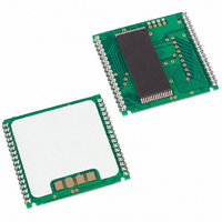
... This design allows the PowerCap to be mounted on top of the DS1644P after the completion of the surface-mount process. Mounting the PowerCap after the surface mount process prevents damage to the crystal and battery due to the high temperatures required for solder reflow ...
Page 4
... Clock accuracy is also affected by the electrical environment and caution should be taken to place the RTC in the lowest level EMI section of the PCB layout. For additional information please see application note 58. bit is the MSB for the seconds registers. Setting it to OSC DS1644/DS1644P ...
Page 5
... The start of a write must return inactive for a minimum prior to the end of write and remain valid for t DS signal will be high during a write cycle. However, OE after WE WEZ DS1644/DS1644P FUNCTION — — Year — — Month — — ...
Page 6
... DS1644 can be accessed as described above with CC is below the power-fail point V CC signal. At this time the power-fail output signal ( CE returns to nominal levels. When DS1644/DS1644P (point at which write PF ) will be PFO falls below the CC pin to the internal battery and CC ...
Page 7
... OUT Output Logic 0 Voltage (I = +2.1 mA) OUT Power-Fail Voltage SYMBOL MIN -0.3 IL SYMBOL MIN I CC1 I ) CC2 CC3 2 4 DS1644/DS1644P (Over the Operating Range) TYP MAX UNITS NOTES 5 +0 0.8 V (Over the Operating Range) TYP MAX UNITS NOTES 4.0 mA A +1 0 ...
Page 8
... WEW t WEZ DH1 t 15 DH2 SYMBOL MIN SYMBOL MIN Fall Time t 300 Rise Time REC DS1644/DS1644P (Over the Operating Range) TYP MAX UNITS NOTES ns 120 ns 120 100 +25C) A TYP MAX UNITS NOTES (Over the Operating Range) TYP MAX UNITS NOTES s ...
Page 9
... DS1644 READ CYCLE TIMING DS1644 WRITE CYCLE TIMING DS1644/DS1644P ...
Page 10
... POWER-DOWN/POWER-UP TIMING OUTPUT LOAD DS1644/DS1644P ...
Page 11
... RoHS status only. Package drawings may show a different suffix character, but the drawing pertains to the package regardless of RoHS status. PACKAGE TYPE 28 EDIP 34 PWRCP th week of 1992. going high. WE going high. CE PACKAGE CODE MDF28+3 PC2 DS1644/DS1644P Note DOCUMENT NO. 21-0245 21-0246 ...
Page 12
... SECONDS. TO SOLDER, APPLY FLUX TO THE PAD, HEAT THE LEAD FRAME PAD AND APPLY SOLDER. TO REMOVE THE PART, APPLY FLUX, HEAT THE LEAD FRAME PAD UNTIL THE SOLDER REFLOWS AND USE A SOLDER WICK TO REMOVE SOLDER DS1644/DS1644P NOM MAX 0.925 0.930 0.985 0.990 - 0 ...
Page 13
... DS1644P WITH DS9034PCX ATTACHED RECOMMENDED POWERCAP MODULE LAND PATTERN PKG INCHES DIM MIN A 0.920 B 0.955 C 0.240 D 0.052 E 0.048 F 0.015 G 0.020 PKG INCHES DIM MIN DS1644/DS1644P NOM MAX 0.925 0.930 0.960 0.965 0.245 0.250 0.055 0.058 0.050 0.052 0.020 0.025 0.025 0.030 ...
Page 14
... Maxim cannot assume responsibility for use of any circuitry other than circuitry entirely embodied in a Maxim product. No circuit patent licenses are implied. Maxim reserves the right to change the circuitry and specifications without notice at any time © 2010 Maxim Integrated Products DESCRIPTION Maxim and the Dallas logo are registered trademarks of Maxim Integrated Products, Inc. DS1644/DS1644P PAGES CHANGED 1, 7 ...