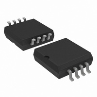
PCF8583T/5,512 NXP Semiconductors, PCF8583T/5,512 Datasheet - Page 17

PCF8583T/5,512
Manufacturer Part Number
PCF8583T/5,512
Description
IC CLK/CALENDAR 240X8 RAM 8-SOIC
Manufacturer
NXP Semiconductors
Type
Clock/Calendar/NVSRAMr
Datasheet
1.PCF8583BS518.pdf
(37 pages)
Specifications of PCF8583T/5,512
Package / Case
8-SOIC (7.5mm Width)
Time Format
HH:MM:SS (12/24 hr)
Memory Size
240B
Date Format
YY-MM-DD
Interface
I²C, 2-Wire Serial
Voltage - Supply
1 V ~ 6 V
Operating Temperature
-40°C ~ 85°C
Mounting Type
Surface Mount
Function
Clock, Calendar, Alarm, Timer Interrupt
Rtc Memory Size
240 B
Supply Voltage (max)
6 V
Supply Voltage (min)
2.5 V
Maximum Operating Temperature
+ 85 C
Minimum Operating Temperature
- 40 C
Mounting Style
SMD/SMT
Rtc Bus Interface
Serial
Lead Free Status / RoHS Status
Lead free / RoHS Compliant
Other names
935276539512
PCF8583TD
PCF8583TD
PCF8583TD
PCF8583TD
NXP Semiconductors
PCF8583
Product data sheet
8.2.1 Addressing
8.2.2 Clock and calendar READ or WRITE cycles
8.2 I
Before any data is transmitted on the I
addressed first. The addressing is always carried out with the first byte transmitted after
the start procedure.
The clock and calendar acts as a slave receiver or slave transmitter. The clock signal SCL
is only an input signal but the data signal SDA is a bidirectional line.
The clock and calendar slave address is shown in
hardware address pin A0. Connecting this pin to V
of two different addresses.
Table 5.
The I
Figure
Bit
2
Fig 18. Master transmits to slave receiver (WRITE mode)
C-bus protocol
2
C-bus configuration for the different PCF8583 READ and WRITE cycles is shown in
18,
Slave address
7
MSB
1
Figure 19
S
I
2
C slave address byte
SLAVE ADDRESS
All information provided in this document is subject to legal disclaimers.
6
0
and
Rev. 06 — 6 October 2010
Figure
acknowledgement
R/W
from slave
0 A
5
1
20.
REGISTER ADDRESS A
2
C-bus, the device which must respond is
4
0
Clock and calendar with 240 x 8-bit RAM
acknowledgement
from slave
DD
3
0
Table
or V
5. Bit A0 corresponds to
SS
n bytes
allows the device to have one
2
0
DATA
memory register address
auto increment
acknowledgement
from slave
1
A0
PCF8583
© NXP B.V. 2010. All rights reserved.
A
013aaa346
P
0
LSB
R/W
17 of 37


