DP8573AV/NOPB National Semiconductor, DP8573AV/NOPB Datasheet - Page 2
DP8573AV/NOPB
Manufacturer Part Number
DP8573AV/NOPB
Description
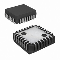
IC REAL TIME CLOCK (RTC) 28-PLCC
Manufacturer
National Semiconductor
Type
Clock/Calendar/NVSRAMr
Series
-r
Datasheet
1.DP8573AVXNOPB.pdf
(16 pages)
Specifications of DP8573AV/NOPB
Memory Size
32B
Time Format
HH:MM:SS:hh (12/24 hr)
Date Format
YY-MM-DD-dd
Interface
Parallel
Voltage - Supply
4.5 V ~ 5.5 V
Operating Temperature
-40°C ~ 85°C
Mounting Type
Surface Mount
Package / Case
28-PLCC
Features
Alarm, Leap Year
Voltage - Supply, Battery
2.2 V ~ 5.1 V
Lead Free Status / RoHS Status
Contains lead / RoHS non-compliant
Other names
*DP8573AV
*DP8573AV/NOPB
DP8573AV
*DP8573AV/NOPB
DP8573AV
Available stocks
Company
Part Number
Manufacturer
Quantity
Price
Company:

Part Number:
DP8573AV/NOPB
Manufacturer:
Renesas
Quantity:
207
Company:
Part Number:
DP8573AV/NOPB
Manufacturer:
Texas Instruments
Quantity:
10 000


Absolute Maximum Ratings
If Military Aerospace specified devices are required
please contact the National Semiconductor Sales
Office Distributors for availability and specifications
Supply Voltage (V
DC Input Voltage (V
DC Output Voltage (V
Storage Temperature Range
Power Dissipation (PD)
Lead Temperature (Soldering 10 sec )
DC Electrical Characteristics
V
Note 1 Absolute Maximum Ratings are those values beyond which damage to the device may occur
Note 2 Unless otherwise specified all voltages are referenced to ground
Note 3 In battery backed mode V
Note 4 This parameter (V
Note 5 This specification tests I
Note 6 This specification tests I
Note 7 OSC IN is driven by a signal generator Contents of the Test Register
Symbol
V
V
V
V
I
I
I
I
I
I
I
IN
OZ
LKG
CC
CC
BB
BLK
CC
IH
IL
OH
OL
e
Single Supply Mode Data retention voltage is 2 2V min
In single Supply Mode (Power connected to V
5V
g
10% V
High Level Input Voltage
(Note 4)
Low Level Input Voltage
High Level Output Voltage
(Excluding OSC OUT)
Low Level Output Voltage
(Excluding OSC OUT)
Input Current (Except OSC IN)
Output TRI-STATE Current
Output High Leakage Current
T1 MFO INTR Pins
Quiescent Supply Current
(Note 6)
Quiescent Supply Current
(Single Supply Mode)
(Note 7)
Standby Mode Battery
Supply Current
(Note 7)
Battery Leakage
CC
IN
)
IH
BB
OUT
)
) is not tested on all pins at the same time
e
)
CC
CC
Parameter
3V V
BB s
with all power fail circuitry disabled by setting D7 of Interrupt Control Register 1 to 0
with all power fail circuitry enabled by setting D7 of Interrupt Control Register 1 to 1
V
PFAIL l
CC
b
b
b
0 4V
0 5V to V
0 5V to V
b
V
CC
b
65 C to
IH
0 5V to
pin) 4 5V
C
(Notes 1
L
CC
CC
e
a
500 mW
a
a
a
100 pF (unless otherwise specified)
s
150 C
260 C
Any Inputs Except OSC IN
OSC IN with External Clock
All Inputs Except OSC IN
OSC IN with External Clock
I
I
I
I
V
V
V
Outputs Open Drain
F
V
V
V
V
V
F
V
OSC OUT
other pins
F
2 2V
other pins at GND
V
V
7 0V
0 5V
0 5V
OUT
OUT
OUT
OUT
V
OSC
OSC
OSC
IN
OUT
OUT
IN
IN
IN
BB
IN
CC
CC
CC
CC s
2)
e
e
e
e
e
e
e
e
e
s
e b
e b
e
e
e
e
e
e
e
V
V
V
V
V
5 5V
GND
GND
GND
5 5V
V
Conditions
20 A
4 0 mA
e
CC
CC
CC
IH
CC
2
32 768 kHz
32 768 kHz
32 768 kHz
V
V
BB s
20 A
4 0 mA
CC
CC
e
00(H) and the MFO pin is not configured as buffered oscillator out
or V
e
or GND
or GND (Note 5)
or GND (Note 6)
or GND
Operation Conditions
Supply Voltage (V
Supply Voltage (V
DC Input or Output Voltage
Operation Temperature (T
Electr-Static Discharge Rating
Transistor Count
Typical Values
GND
open circuit
or GND
or GND
IL
4 0V
(V
JA
JA
(Note 6)
IN
DIP
PLCC Board
V
OUT
)
Board
Socket
Socket
CC
BB
) (Note 3)
) (Note 3)
V
V
BB
CC
Min
b
A
2 0
3 5
)
b
b
5
0 1
0 1
b
Min
4 5
2 2
0 0
40
g
g
g
Max
0 25
12 0
250
0 8
0 1
0 1
1 0
1 5
40
10
V
1 0
5 0
5 0
59 C W
65 C W
80 C W
88 C W
10 300
CC
Max
a
V
5 5
CC
1
b
85
0 4
Units
mA
mA
Unit
V
V
V
V
V
V
V
V
kV
A
A
A
A
A
A
A
A
V
V
V
C
Related parts for DP8573AV/NOPB
Image
Part Number
Description
Manufacturer
Datasheet
Request
R

Part Number:
Description:
Clock IC
Manufacturer:
National Semiconductor
Datasheet:

Part Number:
Description:
National Semiconductor [8-Bit D/A Converter]
Manufacturer:
National Semiconductor
Datasheet:
Part Number:
Description:
National Semiconductor [Media Coprocessor]
Manufacturer:
National Semiconductor
Datasheet:
Part Number:
Description:
Digitally Controlled Tone and Volume Circuit with Stereo Audio Power Amplifier, Microphone Preamp Stage and National 3D Sound
Manufacturer:
National Semiconductor
Datasheet:
Part Number:
Description:
Digitally Controlled Tone and Volume Circuit with Stereo Audio Power Amplifier, Microphone Preamp Stage and National 3D Sound
Manufacturer:
National Semiconductor
Datasheet:
Part Number:
Description:
AC97 Rev 2 Codec with Sample Rate Conversion and National 3D Sound
Manufacturer:
National Semiconductor
Part Number:
Description:
Manufacturer:
National Semiconductor
Datasheet:
Part Number:
Description:
Manufacturer:
National Semiconductor
Datasheet:
Part Number:
Description:
General Purpose, Low Voltage, Low Power, Rail-to-Rail Output Operational Amplifiers
Manufacturer:
National Semiconductor
Datasheet:
Part Number:
Description:
8-bit 20 MSPS flash A/D converter.
Manufacturer:
National Semiconductor
Datasheet:
Part Number:
Description:
Low Noise Quad Operational Amplifier
Manufacturer:
National Semiconductor
Datasheet:
Part Number:
Description:
Quad Differential Line Receivers
Manufacturer:
National Semiconductor
Datasheet:
Part Number:
Description:
Quad High Speed Trapezoidal? Bus Transceiver
Manufacturer:
National Semiconductor
Datasheet:
Part Number:
Description:
Dual Line Receiver
Manufacturer:
National Semiconductor
Datasheet: