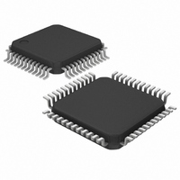
DS1558W+TRL Maxim Integrated Products, DS1558W+TRL Datasheet - Page 6

DS1558W+TRL
Manufacturer Part Number
DS1558W+TRL
Description
IC RTC W/NV RAM 3.3V 48-LQFP
Manufacturer
Maxim Integrated Products
Type
Watchdog Timer/NVSRAMr
Datasheet
1.DS1558W.pdf
(18 pages)
Specifications of DS1558W+TRL
Time Format
HH:MM:SS (24 hr)
Date Format
YY-MM-DD-dd
Interface
Parallel
Voltage - Supply
3 V ~ 3.6 V
Operating Temperature
-40°C ~ 85°C
Mounting Type
Surface Mount
Package / Case
48-LQFP
Lead Free Status / RoHS Status
Lead free / RoHS Compliant
Memory Size
-
DATA WRITE MODE
The DS1558 is in the write mode whenever
referenced to the latter occurring transition of
the cycle.
read or write cycle. Data in must be valid t
afterward. In a typical application, the
provided that care is taken with the data bus to avoid bus con
transitioning low, the data bus can become active with read data defined by the add
transition on
DATA RETENTION MODE
The 5V device is fully accessible and data can be written and read only when V
However, when V
internal clock registers and SRAM are blocked from any access. When V
point V
operation and SRAM data are maintained from the battery until V
The 3.3V device is fully accessible and data can be written and read only when V
When V
switched from V
than V
below V
nominal levels.
All control, data, and address signals must be powered down when V
BATTERY LONGIVITY
The battery lifetime is dependent on the RAM battery standby current and the DS1
oscillator current. The total battery current is I
50nA. The DS1558 has an internal circuit to prevent battery chargin
are required, and none should be used. The DS1558 has two battery pins that operate independently; the
DS1558 selects the higher of the two inputs. If only one battery is used, the battery should be attached to
V
INTERNAL BATTERY MONITOR
The DS1558 constantly monitors the battery voltage of the internal battery. The battery-low flag (BLF)
bit of the flags register (B4 of 7FFF0h) is not writable and should always be a 0 when read. If a 1 is ever
present, both battery inputs are below 1.8V and both the contents of the RTC and RAM are questionable.
POWER-ON RESET
A temperature-compensated comparator circuit monitors the level of V
fail trip point, the
signal continues to be pulled low for a period of 40ms to 200ms. The power-on reset function is
independent of the RTC oscillator and thus is operational whether or not the oscillator is enabled.
BAT1
, and V
SO
SO
CC
SO
, the device power is switched from V
(battery supply level), device power is switched from the V
CE
. RTC operation and SRAM data are maintained from the battery until
falls below V
BAT2
WE
and
C
then disables the outputs t
should be grounded.
C
CC
RST
WE
t
o the internal backup lithium battery when V
is below the power-fail point V
must return inactive for a minimum of t
signal (open drain) is pulled low. When V
PF
, access to the device is inhibited. If V
OE
signal is high during a write cycle. However,
WEZ
WE
OSC
DS
WE
CC
after
prior to the
+ I
6 of 18
and
to the internal backup lithium battery when V
or
CCO
WE
CE
CE
PF
. When V
goes active.
. The addresses must be hel
are in their active state. The
(point at which write prot
end of the write and remain valid for t
WR
CC
CC
PF
CC
CC
prior to the initiation of a subsequent
g. No external protection components
ten
is returned to nom
is above V
is less than V
CC
returns to nominal levels, the
drops below V
tion.
CC
is powered down.
CC
CC
pin to the backup battery. RTC
. When V
falls below the batter
If
PF
OE
, I
SO
CC
BAT
CC
CC
is low prior to
, t
PF
i
i
ection occurs), the
s greater than V
inal levels.
he device power is
V
ress inputs. A low
d valid throughout
s greater than V
558 internal clock
current is less than
falls to the power-
. If V
start of a write is
CC
OE
is returned to
can be active
PF
is greater
CC
y switch
drops
RST
WE
DH
PF
PF
.
.


