DS1284Q Maxim Integrated Products, DS1284Q Datasheet
DS1284Q
Specifications of DS1284Q
Available stocks


Related parts for DS1284Q

DS1284Q Summary of contents
Page 1
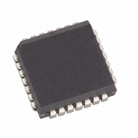
... PLCC/Tape and Reel 5.0 28 PLCC/Tape and Reel 5.0 28 EDIP (720 mils) 5.0 28 EDIP (720 mils) 5.0 28 EDIP (720 mils DS1284/DS1286 Watchdog Timekeepers CC TOP MARK* DS1284 DS1284 N DS1284Q DS1284Q DS1284Q DS1284Q DS1284QN DS1284QN DS1284QN DS1284QN DS1286 DS1286 IND DS1286 IND REV: 032406 ...
Page 2
OPERATION—READ REGISTERS The DS1284/DS1286 execute a read cycle whenever WE (write enable) is inactive (high) and CE (chip enable) and OE (output enable) are active (low). The unique address specified by the six address inputs (A0–A5) defines which of the ...
Page 3
PIN DESCRIPTION PIN DIP EDIP PLCC — 21, 24 5–10 5–10 5–10 11, 12, 11, 12, 11, 12, 13, 15, 13, 15, 13, 15, 16–19 16–19 16–19 ...
Page 4
PIN DIP EDIP PLCC Figure 1. Block Diagram X1 8 Oscillator X2 DS1286 only Internal Registers External Registers, clock, calendar, time of day alarm Command Register A0-A5 CE User RAM 50 Bytes OE WE NAME Primary ...
Page 5
HUNDREDTHS-OF-SECONDS GENERATOR The hundredths-of-seconds generator circuit shown in the Block Diagram (Figure state machine that divides the incoming frequency (4096Hz for 24 cycles and 40 for 1 cycle. This produces a 100Hz output that is ...
Page 6
TIME-OF-DAY REGISTERS Registers and A contain time-of-day data in BCD. Ten bits within these eight registers are not used and always read 0 regardless of how they are written. Bits 6 and 7 ...
Page 7
WATCHDOG ALARM REGISTERS Registers C and D contain the time for the watchdog alarm. The two registers contain a time count from to 99.99 seconds in BCD. The value written into the watchdog alarm registers can be written or read ...
Page 8
Bit 1: Watchdog Alarm Flag (WAF). When this bit is set internally to logic 1, a watchdog alarm has ...
Page 9
ABSOLUTE MAXIMUM RATINGS Voltage Range on Any Pin Relative to Ground……………………………………………..-0.3V to +7.0V Operating Temperature Range Commercial………………………………………………………………………………..0C to +70C Industrial………………………………………………………………………………...-40°C to +85°C Storage Temperature Range………………………………………………………………...-40°C to +85°C Soldering Temperature………………..……………...See IPC/JEDEC J-STD-020 Specification (Note 13) Stresses beyond those listed as “Absolute ...
Page 10
CAPACITANCE (T = +25°C) A PARAMETER Input Capacitance Output Capacitance Input/Output Capacitance AC ELECTRICAL CHARACTERISTICS (V = 4.5V to 5.5V -40C to +85C or 0°C to +70°C PARAMETER Read Cycle Time Address Access Time CE Access ...
Page 11
READ CYCLE (NOTE 1) WRITE CYCLE 1 (NOTES DS1284/DS1286 ...
Page 12
WRITE CYCLE 2 (NOTES 2, 8) TIMING DIAGRAM: INTERRUPT OUTPUTS PULSE MODE (NOTES 11, 12 DS1284/DS1286 ...
Page 13
POWER-UP/POWER-DOWN CONDITION PARAMETER before Power-Down IH V Slew from 4. ( Slew from 0V to 4.5V ( after Power-Up IH POWER-DOWN/POWER-UP CONDITION (T = +25°C) ...
Page 14
NOTES high for a read cycle specified as the logical AND of CE and WE low to the earlier ...
Page 15
PIN CONFIGURATIONS TOP VIEW INTA DS1284 3 N. DQ0 11 12 DQ1 13 DQ2 14 GND DIP (600 mils) INTA ...
Page 16
PACKAGE INFORMATION PKG 28-PIN PLCC DIM MIN A IN. 0.300 BSC MM 7.62 B IN. 0.442 MM 17.68 D IN. 0.480 MM 12.2 D2 IN. 0.390 MM 9.91 E IN. 0.090 MM 2.29 E2 IN. 0.390 MM 9.91 F IN. ...
Page 17
PACKAGE INFORMATION (continued) PKG 28-PIN DIP DIM MIN A IN. 1.445 MM B IN. 0.530 MM C IN. 0.140 MM D IN. 0.600 MM E IN. 0.015 MM F IN. 0.120 MM G IN. 0.090 MM H IN. 0.625 MM ...
Page 18
... Maxim/Dallas Semiconductor cannot assume responsibility for use of any circuitry other than circuitry entirely embodied in a Maxim/Dallas Semiconductor product. No circuit patent licenses are implied. Maxim/Dallas Semiconductor reserves the right to change the circuitry and specifications without notice at any time The Maxim logo is a registered trademark of Maxim Integrated Products, Inc. The Dallas logo is a registered trademark of Dallas Semiconductor Corporation. PKG DIM A IN ...