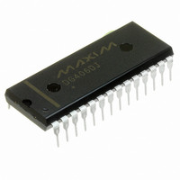
DS1284 Maxim Integrated Products, DS1284 Datasheet - Page 2

DS1284
Manufacturer Part Number
DS1284
Description
IC TIMEKEEPER WATCHDOG 28-DIP
Manufacturer
Maxim Integrated Products
Type
Watchdog Timerr
Datasheet
1.DS1284QN.pdf
(18 pages)
Specifications of DS1284
Memory Size
50B
Time Format
HH:MM:SS:hh (12/24 hr)
Date Format
YY-MM-DD-dd
Interface
Parallel
Voltage - Supply
4.5 V ~ 5.5 V
Operating Temperature
0°C ~ 70°C
Mounting Type
Through Hole
Package / Case
28-DIP (0.600", 15.24mm)
Lead Free Status / RoHS Status
Contains lead / RoHS non-compliant
Available stocks
Company
Part Number
Manufacturer
Quantity
Price
Company:
Part Number:
DS1284Q
Manufacturer:
DALLAS
Quantity:
5 510
Part Number:
DS1284Q
Manufacturer:
N/A
Quantity:
20 000
Company:
Part Number:
DS1284Q+T&R
Manufacturer:
Maxim Integrated
Quantity:
10 000
Company:
Part Number:
DS1284Q/T&R
Manufacturer:
Maxim Integrated
Quantity:
10 000
Part Number:
DS1284Q/TR
Manufacturer:
DALLAS
Quantity:
20 000
Company:
Part Number:
DS1284QN
Manufacturer:
DALLAS
Quantity:
5 510
Company:
Part Number:
DS1284QN
Manufacturer:
WALL
Quantity:
5 510
OPERATION—READ REGISTERS
The DS1284/DS1286 execute a read cycle whenever WE (write enable) is inactive (high) and CE (chip
enable) and OE (output enable) are active (low). The unique address specified by the six address inputs
(A0–A5) defines which of the 64 registers is to be accessed. Valid data is available to the eight data
output drivers within t
OE access times are also satisfied. If OE and CE access times are not satisfied, then data access must be
measured from the latter occurring signal (CE or OE) and the limiting parameter is either t
for OE rather than address access.
OPERATION—WRITE REGISTERS
The DS1284/DS1286 are in the write mode whenever the WE and CE signals are in the active-low state
after the address inputs are stable. The latter occurring falling edge of CE or WE determines the start of
the write cycle. The write cycle is terminated by the earlier rising edge of CE or WE. All address inputs
must be kept valid throughout the write cycle. WE must return to the high state for a minimum recovery
state (t
setup (t
signal should be kept inactive (high) during write cycles to avoid bus contention. However, if the output
bus has been enabled (CE and OE active), then WE will disable the outputs in t
DATA RETENTION
The watchdog timekeeper provides full functional capability when V
maintained in the absence of V
constantly monitor V
protects itself, and all inputs to the registers become “don’t care.” Both INTA and INTB (INTB) are
open-drain outputs. The two interrupts and the internal clock continue to run regardless of the level of
V
pulled up to a value greater than V
circuit turns on the lithium energy source to maintain the clock and timer data functionality. Also ensure
that during this time (battery-backup mode), the voltage present at INTA and INTB (INTB) never
exceeds the battery voltage. If the active-high mode is selected for INTB (INTB), this pin only goes high
in the presence of V
circuit connects external V
V
WATCHDOG TIMEKEEPER REGISTERS
The watchdog timekeeper has 64 8-bits-wide registers that contain all the timekeeping, alarm, watchdog,
control, and data information. The clock, calendar, alarm, and watchdog registers are memory locations
that contain external (user-accessible) and internal copies of the data. The external copies are independent
of internal functions, except that they are updated periodically by the simultaneous transfer of the
incremented internal copy (see Figure 1). The command register bits are affected by both internal and
external functions. This register is discussed later. The 50 bytes of RAM registers can only be accessed
from the external address and data bus. Registers 0, 1, 2, 4, 6, 8, 9, and A contain time-of-day and date
information (see Figure 2). Time-of-day information is stored in binary-coded decimal (BCD). Registers
3, 5, and 7 contain the time-of-day alarm information. Time-of-day alarm information is stored in BCD.
Register B is the command register and information in this register is binary. Registers C and D are the
watchdog alarm registers and information stored in these two registers is in BCD. Registers E to 3F are
user bytes and can be used to contain data at the user’s discretion.
CC
CC
. However, it is important to ensure that the pullup resistors used with the interrupt pins are never
exceeds V
WR
DS
) before another cycle can be initiated. Data must be valid on the data bus with sufficient data
) and data hold time (t
TP
for t
CC
REC
CC
. During power-up, when V
ACC
. Should the supply voltage decay, the watchdog timekeeper automatically write
.
(access time) after the last address input signal is stable, provided that CE and
CC
and disconnects the V
DH
) with respect to the earlier rising edge of CE or WE. The OE control
CC
CC
+ 0.3V. As V
without any additional support circuitry. The DS1284/DS1286
CC
2 of 18
BAT
CC
rises above approximately 3.0V, the power-switching
falls below the battery voltage, a power-switching
energy source. Normal operation can resume after
CC
is greater than V
ODW
from its falling edge.
CO
DS1284/DS1286
for CE or t
TP
. Data is
OE


