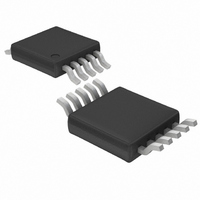
LTC2411IMS#PBF Linear Technology, LTC2411IMS#PBF Datasheet - Page 9

LTC2411IMS#PBF
Manufacturer Part Number
LTC2411IMS#PBF
Description
IC A/D CONV 24BIT MICRPWR 10MSOP
Manufacturer
Linear Technology
Datasheet
1.LTC2411CMSPBF.pdf
(40 pages)
Specifications of LTC2411IMS#PBF
Number Of Bits
24
Sampling Rate (per Second)
7.5
Data Interface
MICROWIRE™, Serial, SPI™
Number Of Converters
2
Power Dissipation (max)
1mW
Voltage Supply Source
Single Supply
Operating Temperature
-40°C ~ 85°C
Mounting Type
Surface Mount
Package / Case
10-TFSOP, 10-MSOP (0.118", 3.00mm Width)
Number Of Elements
1
Resolution
24Bit
Architecture
Delta-Sigma
Sample Rate
0.008KSPS
Input Polarity
Bipolar
Input Type
Voltage
Rated Input Volt
±2.75V
Differential Input
Yes
Power Supply Requirement
Single
Single Supply Voltage (typ)
3.3/5V
Single Supply Voltage (min)
2.7V
Single Supply Voltage (max)
5.5V
Dual Supply Voltage (typ)
Not RequiredV
Dual Supply Voltage (min)
Not RequiredV
Dual Supply Voltage (max)
Not RequiredV
Integral Nonlinearity Error
14ppm of Vref
Operating Temp Range
-40C to 85C
Operating Temperature Classification
Industrial
Mounting
Surface Mount
Pin Count
10
Package Type
MSOP
Input Signal Type
Differential
Lead Free Status / RoHS Status
Lead free / RoHS Compliant
Available stocks
Company
Part Number
Manufacturer
Quantity
Price
V
(Pin 6) with a 10 F tantalum capacitor in parallel with
0.1 F ceramic capacitor as close to the part as possible.
REF
The voltage on these pins can have any value between GND
and V
more positive than the reference negative input, REF
at least 0.1V.
IN
voltage on these pins can have any value between
TYPICAL PERFOR A CE CHARACTERISTICS
PI FU CTIO S
CC
–100
–120
210
230
220
200
190
180
170
160
–20
–40
–60
–80
+
240
40
20
U
0
–45
+
(Pin 4), IN
(Pin 1): Positive Supply Voltage. Bypass to GND
Conversion Current
vs Temperature
0
Offset Error vs Output Data Rate
(Pin 2), REF
CC
F
CS = GND
SCK = NC
SDO = NC
V
REF
V
V
F
T
O
O
A
CC
INCM
IN
–30
10
= GND
= EXT OSC
= 25 C
OUTPUT DATA RATE (READINGS/SEC)
= 0V
as long as the reference positive input, REF
–
= 5V
= GND
U
= 2.5V
20
–15
30
TEMPERATURE ( C)
0
–
40
(Pin 5): Differential Analog Input. The
15
–
50
(Pin 3): Differential Reference Input.
U
V
30
REF
60
V
V
V
V
V
REF
CC
CC
= 2.5V
45
CC
CC
70
= 5.5V
= 2.7V
= 5V
= 5V
= 3V
W
60
80
75
2411 G25
90
2411 G28
U
100
90
650
600
550
500
450
400
350
300
250
200
150
22
21
20
19
18
0
0
Conversion Current
vs Output Data Rate
Resolution (NOISE
vs Output Data Rate
REF
REF
IN
IN
T
SCK = NC
SDO = NC
CS = GND
F
V
REF
V
V
F
RES = LOG
T
A
O
O
A
CC
INCM
IN
+
–
10
= 25 C
= EXT OSC
10
OUTPUT DATA RATE (READINGS/SEC)
= EXT OSC
= 25 C
OUTPUT DATA RATE (READINGS/SEC)
+
–
= GND
= GND
= 0V
–
= 5V
= V
= GND
= GND
= 2.5V
20
20
CC
–
+
, by
2
, is
30
(V
30
REF
40
40 50
/NOISE
V
V
REF
REF
50
GND – 0.3V and V
converter bipolar input range (V
from – 0.5 • (V
range, the converter produces unique overrange and
underrange output codes.
GND (Pin 6): Ground. Connect this pin to a ground plane
through a low impedance connection.
CS (Pin 7): Active LOW Digital Input. A LOW on this pin
enables the SDO digital output and wakes up the ADC.
Following each conversion the ADC automatically enters
V
V
= 2.5V
RMS
CC
= 5V
RMS
CC
60 70
60
= 5V
= 3V
)
70
1LSB)
80
80
90
90
2411 G26
2411 G29
100
100
REF
LTC2411/LTC2411-1
) to 0.5 • (V
CC
22
20
18
16
14
12
10
+ 0.3V. Within these limits, the
3
2
0
5
4
1
–45
0
Sleep Mode Current
vs Temperature
Resolution (INL
vs Output Data Rate
V
REF
V
V
F
RES = LOG
T
O
CC
INCM
IN
A
–30
10
= EXT OSC
= 25 C
OUTPUT DATA RATE (READINGS/SEC)
–
= 0V
= 5V
= GND
= 2.5V
20
–15
REF
IN
2
30
(V
TEMPERATURE ( C)
0
REF
= IN
). Outside this input
40
/INL
15
MAX
V
50
+
MAX
REF
30
– IN
)
60
= 2.5V
V
V
V
V
CC
CC
1LSB)
45
CC
CC
70
–
= 5.5V
= 2.7V
= 5V
= 3V
V
) extends
F
CS = V
SCK = NC
SDO = NC
60
REF
O
80
= GND
= 5V
75
2411 G27
90
CC
2411 G30
9
100
90


