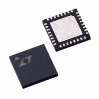
LTC2351IUH-14#PBF Linear Technology, LTC2351IUH-14#PBF Datasheet - Page 3

LTC2351IUH-14#PBF
Manufacturer Part Number
LTC2351IUH-14#PBF
Description
IC ADC 14BIT 1.5MSPS 32-QFN
Manufacturer
Linear Technology
Datasheet
1.LTC2351IUH-14PBF.pdf
(20 pages)
Specifications of LTC2351IUH-14#PBF
Number Of Bits
14
Sampling Rate (per Second)
1.5M
Data Interface
Serial, SPI™
Number Of Converters
1
Power Dissipation (max)
16.5mW
Voltage Supply Source
Single Supply
Operating Temperature
-40°C ~ 85°C
Mounting Type
Surface Mount
Package / Case
32-WFQFN Exposed Pad
Number Of Elements
1
Resolution
14Bit
Sample Rate
1.5MSPS
Input Polarity
Unipolar/Bipolar
Input Type
Voltage
Rated Input Volt
2.5/±1.25V
Differential Input
Yes
Power Supply Requirement
Analog and Digital
Single Supply Voltage (typ)
3V
Single Supply Voltage (min)
2.7V
Single Supply Voltage (max)
3.6V
Dual Supply Voltage (typ)
Not RequiredV
Dual Supply Voltage (min)
Not RequiredV
Dual Supply Voltage (max)
Not RequiredV
Power Dissipation
100mW
Differential Linearity Error
1LSB(Typ)
Integral Nonlinearity Error
±3LSB
Operating Temp Range
-40C to 85C
Operating Temperature Classification
Industrial
Mounting
Surface Mount
Pin Count
32
Package Type
QFN EP
Lead Free Status / RoHS Status
Lead free / RoHS Compliant
Available stocks
Company
Part Number
Manufacturer
Quantity
Price
DYNAMIC ACCURACY
DIGITAL INPUTS AND DIGITAL OUTPUTS
ANALOG INPUT
otherwise specifi cations are at T
SYMBOL
SINAD
THD
SFDR
IMD
INTERNAL REFERENCE CHARACTERISTICS
PARAMETER
V
V
V
V
V
External V
full operating temperature range, otherwise specifi cations are at T
SYMBOL
V
V
otherwise specifi cations are at T
SYMBOL
V
V
I
C
t
t
t
t
CMRR
IN
ACQ
AP
JITTER
SK
IN
CM
IN
REF
REF
REF
REF
REF
IH
IL
Output Voltage
Output Tempco
Line Regulation
Output Resistance
Settling Time
REF
PARAMETER
Analog Differential Input Range (Notes 3, 8, 9)
Analog Common Mode + Differential
Input Range
Analog Input Leakage Current
Analog Input Capacitance
Sample-and-Hold Acquisition Time
Sample-and-Hold Aperture Delay Time
Sample-and-Hold Aperture Delay Time Jitter
Channel to Channel Aperture Skew
Analog Input Common Mode Rejection Ratio
PARAMETER
Signal-to-Noise Plus
Distortion Ratio
Total Harmonic
Distortion
Spurious Free
Dynamic Range
Intermodulation
Distortion
Code-to-Code
Transition Noise
Full Power Bandwidth
Full Linear Bandwidth
Input Range
PARAMETER
High Level Input Voltage
Low Level Input Voltage
The
A
A
CONDITIONS
100kHz Input Signal
300kHz Input Signal
100kHz Input Signal (LTC2351H-14)
100kHz First 5 Harmonics
300kHz First 5 Harmonics
100kHz First 5 Harmonics (LTC2351H-14)
100kHz Input Signal
300kHz Input Signal
0.625V
Bipolar Mode. Also Applicable to Other Channels
V
V
S/(N + D) ≥ 68dB, Bipolar Differential Input
= 25°C. With internal reference, V
= 25°C. With internal reference, V
REF
IN
l
= 2.5V
= 2.5V (Note 17)
denotes the specifi cations which apply over the full operating temperature range,
CONDITIONS
I
V
Load Current = 0.5mA
Ext C
P-P
OUT
DD
, 833kHz into CH0
The
P-P
= 2.7V to 3.6V, V
= 0
REF
, SDO = 11585LSB
l
= 10μF
denotes the specifi cations which apply over the full operating temperature range,
CONDITIONS
V
V
DD
DD
= 3.3V
= 2.7V
CONDITIONS
2.7V ≤ V
2.7V ≤ V
(Note 8)
(Note 6)
f
f
IN
IN
REF
+
, 0.625V
= 100kHz, V
= 10MHz, V
= 2.5V
P-P
DD
DD
(–3dBFS) (Note 15)
P-P
≤ 3.6V, Unipolar
≤ 3.6V, Bipolar
A
DD
= 25°C. V
DD
, 841kHz into CH0
IN
IN
= 0V to 3V
= V
= V
= 0V to 3V
CC
CC
= 3V.
= 3V.
The
T
DD
A
= 25°C. V
= V
l
CC
–
denotes the specifi cations which apply over the
= 3V.
DD
l
l
= V
l
l
l
l
l
l
CC
= 3V.
MIN
2.55
MIN
2.4
MIN
–80
–79
71
70
MIN
0 to V
LTC2351-14
0 to 2.5
TYP
TYP
600
±1.25
TYP
–90
–86
–89
–80
2.5
0.2
15
0.7
TYP
200
–83
–67
75
75
75
90
86
50
0.3
2
13
5
1
DD
MAX
MAX
MAX
MAX
V
0.6
39
DD
1
LSB
ppm/°C
235114fb
UNITS
UNITS
UNITS
UNITS
3
μV/V
MHz
MHz
RMS
ms
μA
dB
dB
dB
dB
dB
dB
dB
dB
dB
dB
dB
pF
ns
ns
ps
ps
Ω
V
V
V
V
V
V
V


