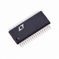
LTC1608CG#PBF Linear Technology, LTC1608CG#PBF Datasheet - Page 14

LTC1608CG#PBF
Manufacturer Part Number
LTC1608CG#PBF
Description
IC A/D CONV 16BIT SAMPLNG 36SSOP
Manufacturer
Linear Technology
Datasheet
1.LTC1608CGPBF.pdf
(20 pages)
Specifications of LTC1608CG#PBF
Number Of Bits
16
Sampling Rate (per Second)
500k
Data Interface
Parallel
Number Of Converters
1
Power Dissipation (max)
420mW
Voltage Supply Source
Analog and Digital, Dual ±
Operating Temperature
0°C ~ 70°C
Mounting Type
Surface Mount
Package / Case
36-SSOP (0.200", 5.30mm Width)
Number Of Elements
1
Resolution
16Bit
Architecture
SAR
Sample Rate
500KSPS
Input Polarity
Bipolar
Input Type
Voltage
Rated Input Volt
±2.5V
Differential Input
Yes
Power Supply Requirement
Dual
Single Supply Voltage (typ)
Not RequiredV
Single Supply Voltage (min)
Not RequiredV
Single Supply Voltage (max)
Not RequiredV
Dual Supply Voltage (typ)
±5V
Dual Supply Voltage (min)
±4.75V
Dual Supply Voltage (max)
±5.25V
Power Dissipation
420mW
Integral Nonlinearity Error
±4LSB
Operating Temp Range
0C to 70C
Operating Temperature Classification
Commercial
Mounting
Surface Mount
Pin Count
36
Package Type
SSOP
Resolution (bits)
16bit
Sampling Rate
500kSPS
Input Channel Type
Differential
Supply Voltage Range - Analogue
± 4.75V To ± 5.25V
Supply Voltage Range - Digital
4.75V To
Rohs Compliant
Yes
Lead Free Status / RoHS Status
Lead free / RoHS Compliant
Available stocks
Company
Part Number
Manufacturer
Quantity
Price
APPLICATIO S I FOR ATIO
Full-Scale and Offset Adjustment
Figure 15a shows the ideal input/output characteristics
for the LTC1608. The code transitions occur midway
between successive integer LSB values (i.e., – FS +
0.5LSB, – FS + 1.5LSB, – FS + 2.5LSB,... FS – 1.5LSB,
FS – 0.5LSB). The output is two’s complement binary with
1LSB = FS – (– FS)/65536 = 5V/65536 = 76.3 V.
In applications where absolute accuracy is important,
offset and full-scale errors can be adjusted to zero. Offset
error must be adjusted before full-scale error. Figure 15b
shows the extra components required for full-scale error
adjustment. Zero offset is achieved by adjusting the offset
applied to the A
– 38 V (i.e., – 0.5LSB) at A
A
the LTC1662 until the output code flickers between 0000
0000 0000 0000 and 1111 1111 1111 1111. For full-scale
adjustment, an input voltage of 2.499886V (FS/2 – 1.5LSBs)
is applied to A
adjusted until the output code flickers between 0111 1111
1111 1110 and 0111 1111 1111 1111.
BOARD LAYOUT AND GROUNDING
Wire wrap boards are not recommended for high resolu-
tion or high speed A/D converters. To obtain the best per-
formance from the LTC1608, a printed circuit board with
LTC1608
Differential inputs allow greater flexibility for accepting
different input ranges. Figure 14b shows a circuit that
converts a 0V to 5V analog input signal with only an
additional buffer that is not in the signal path.
14
IN
–
input by varying the output voltage of pin V
Figure 14b. Selectable 0V to 5V or 2.5V Input Range
2.5V
IN
+
0V TO
5V
IN
ANALOG INPUT
and the output voltage of pin V
–
U
input. For zero offset error, apply
22 F
+
–
U
IN
+
4
5
1
2
3
and adjust the offset at the
A
A
V
REFCOMP
AGND
IN
IN
REF
+
–
W
LTC1608
1608 F14b
U
OUTA
OUTB
from
is
ground plane is required. Layout should ensure that digital
and analog signal lines are separated as much as possible.
Particular care should be taken not to run any digital track
alongside an analog signal track or underneath the ADC.The
analog input should be screened by AGND.
An analog ground plane separate from the logic system
ground should be established under and around the ADC.
Pin 5 to Pin 8 (AGNDs), Pin 10 (ADC’s DGND) and all other
analog grounds should be connected to this single analog
ground point. The REFCOMP bypass capacitor and the
DV
analog ground plane. No other digital grounds should be
connected to this analog ground plane. Low impedance
analog and digital power supply common returns are
essential to low noise operation of the ADC and the foil
width for these tracks should be as wide as possible. In
OFFSET ADJ RANGE: 0.125%
FULL-SCALE ADJ RANGE: 0.25%
5V
DD
bypass capacitor should also be connected to this
CS/LD
SCK
SDI
REF
Figure 15b. Offset and Full-Scale Adjust Circuit
Figure 15a. LTC1608 Transfer Characteristics
LTC1662
011...111
011...110
000...001
000...000
111...111
111...110
100...001
100...000
V
V
0.1 F
OUTA
OUTB
GND
V
– (FS – 1LSB)
CC
INPUT VOLTAGE (A
40.2k
1.5M
R1
R3
–5V
80.6k
1%
+
ANALOG
R2
100
IN
+
2.2 F
INPUT
+
– A
22 F
IN
–
FS – 1LSB
)
4
1
3
5
2
1608 F15a
A
A
V
REFCOMP
AGND
IN
IN
REF
+
–
LTC1608
1608 F15b


