LTC2175IUKG-14#PBF Linear Technology, LTC2175IUKG-14#PBF Datasheet
LTC2175IUKG-14#PBF
Specifications of LTC2175IUKG-14#PBF
Available stocks


Related parts for LTC2175IUKG-14#PBF


LTC2175IUKG-14#PBF Summary of contents
Page 1
... Software Defi ned Radios n Portable Medical Imaging n Multichannel Data Acquisition n Nondestructive Testing L, LT, LTC, LTM, Linear Technology and the Linear logo are registered trademarks of Linear Technology Corporation. All other trademarks are the property of their respective owners. TYPICAL APPLICATION 1. CHANNEL 1 14-BIT ANALOG ...
Page 2
... Operating Temperature Range LTC2175C, 2174C, 2173C ........................ 0°C to 70°C LTC2175I, 2174I, 2173I ....................... –40°C to 85°C Storage Temperature Range ................... –65°C to 150°C ORDER INFORMATION LEAD FREE FINISH TAPE AND REEL LTC2175CUKG-14#PBF LTC2175CUKG-14#TRPBF LTC2175IUKG-14#PBF LTC2175IUKG-14#TRPBF LTC2174CUKG-14#PBF LTC2174CUKG-14#TRPBF LTC2174IUKG-14#PBF LTC2174IUKG-14#TRPBF LTC2173CUKG-14#PBF LTC2173CUKG-14#TRPBF LTC2173IUKG-14#PBF LTC2173IUKG-14#TRPBF Consult LTC Marketing for parts specifi ...
Page 3
CONVERTER CHARACTERISTICS temperature range, otherwise specifi cations are at T PARAMETER CONDITIONS Resolution (No Missing Codes) Integral Linearity Error Differential Analog Input (Note 6) Differential Linearity Error Differential Analog Input Offset Error (Note 7) Gain Error Internal Reference External Reference ...
Page 4
LTC2175-14/ LTC2174-14/LTC2173-14 DYNAMIC ACCURACY otherwise specifi cations are 25° SYMBOL PARAMETER CONDITIONS SNR Signal-to-Noise Ratio 5MHz Input 70MHz Input 140MHz Input SFDR Spurious Free Dynamic Range 5MHz Input 2nd or 3rd Harmonic 70MHz Input 140MHz ...
Page 5
DIGITAL INPUTS AND OUTPUTS temperature range, otherwise specifi cations are at T SYMBOL PARAMETER + – ENCODE INPUTS (ENC , ENC ) – Differential Encode Mode (ENC Not Tied to GND) V Differential Input Voltage ID V Common Mode Input ...
Page 6
LTC2175-14/ LTC2174-14/LTC2173-14 POWER REQUIREMENTS range, otherwise specifi cations are SYMBOL PARAMETER CONDITIONS V Analog Supply Voltage (Note 10 Output Supply Voltage (Note 10 Analog Supply Current Sine Wave Input VDD I Digital Supply ...
Page 7
TIMING CHARACTERISTICS range, otherwise specifi cations are at T SYMBOL PARAMETER SPI Port Timing (Note 8) t SCK Period SCK CS to SCK Setup Time t S SCK to CS Setup Time SDI Setup Time DS t ...
Page 8
LTC2175-14/ LTC2174-14/LTC2173-14 TIMING DIAGRAMS ANALOG INPUT – ENC + ENC – DCO + DCO – – OUT#A + OUT#A – OUT#B + OUT#B *SEE THE DIGITAL OUTPUTS SECTION ANALOG N INPUT – ENC + ENC – DCO ...
Page 9
TIMING DIAGRAMS ANALOG INPUT OUT#A OUT#A OUT#B OUT ANALOG N INPUT – ENC + ENC – DCO + DCO – – OUT D13 D12 D11 D10 + OUT#A SAMPLE ...
Page 10
LTC2175-14/ LTC2174-14/LTC2173-14 TIMING DIAGRAMS t AP ANALOG N INPUT – ENC + ENC – DCO + DCO – – OUT D13 D12 D11 D10 + OUT#A SAMPLE N-6 + – OUT#B ...
Page 11
TYPICAL PERFORMANCE CHARACTERISTICS LTC2175-14: Integral Nonlinearity (INL) 2.0 1.5 1.0 0.5 0 –0.5 –1.0 –1.5 –2.0 0 8192 12288 16384 4096 OUTPUT CODE 217514 G01 LTC2175-14: 8k Point FFT 30MHz IN –1dBFS, 125Msps 0 –10 –20 –30 –40 ...
Page 12
LTC2175-14/ LTC2174-14/LTC2173-14 TYPICAL PERFORMANCE CHARACTERISTICS LTC2175-14: SFDR vs Input Frequency, –1dB, 2V Range, 125Msps 100 150 200 250 300 INPUT FREQUENCY (MHz) 217514 G10 LTC2175-14 Sample Rate, VDD 5MHz ...
Page 13
TYPICAL PERFORMANCE CHARACTERISTICS LTC2174-14: 8k Point FFT 30MHz IN –1dBFS, 105Msps 0 –10 –20 –30 –40 –50 –60 –70 –80 –90 –100 –110 –120 FREQUENCY (MHz) 217514 G17 LTC2174-14: 8k Point 2-Tone ...
Page 14
LTC2175-14/ LTC2174-14/LTC2173-14 TYPICAL PERFORMANCE CHARACTERISTICS LTC2174-14: SNR vs SENSE 5MHz, –1dB 0.6 0.7 0.8 0.9 1 1.1 1.2 1.3 SENSE PIN (V) 217514 G25 LTC2173-14: 8k Point FFT, ...
Page 15
TYPICAL PERFORMANCE CHARACTERISTICS LTC2173-14: SNR vs Input Frequency, –1dB, 2V Range, 80Msps 100 150 200 250 300 350 INPUT FREQUENCY (MHz) 217514 G34 LTC2173-14 Sample Rate, VDD ...
Page 16
LTC2175-14/ LTC2174-14/LTC2173-14 PIN FUNCTIONS + A (Pin 1): Channel 1 Positive Differential Analog IN1 Input. – A (Pin 2): Channel 1 Negative Differential Analog IN1 Input. V (Pin 3): Common Mode Bias Output, Nominally CM12 Equal to V /2. V ...
Page 17
PIN FUNCTIONS become parallel logic inputs that control a reduced set of the A/D operating modes. PAR/SER should be connected directly to ground or the V of the part and not be driven logic signal. V (Pin ...
Page 18
LTC2175-14/ LTC2174-14/LTC2173-14 FUNCTIONAL BLOCK DIAGRAM CH 1 14-BIT S/H ANALOG ADC CORE INPUT CH 2 14-BIT S/H ANALOG ADC CORE INPUT CH 3 14-BIT S/H ANALOG ADC CORE INPUT CH 4 14-BIT S/H ANALOG ADC CORE INPUT V REF 1.25V ...
Page 19
APPLICATIONS INFORMATION CONVERTER OPERATION The LTC2175-14/LTC2174-14/LTC2173-14 are low power, 4-channel, 14-bit, 125Msps/105Msps/80Msps A/D con- verters that are powered by a single 1.8V supply. The analog inputs should be driven differentially. The encode input can be driven differentially for optimal jitter ...
Page 20
LTC2175-14/ LTC2174-14/LTC2173-14 APPLICATIONS INFORMATION tap is biased with V , setting the A/D input at its opti- CM mal DC level. At higher input frequencies a transmission line balun transformer (Figures has better balance, resulting in lower ...
Page 21
APPLICATIONS INFORMATION ground. For a 2V input range with an external reference, apply a 1.25V reference voltage to SENSE (Figure 9). The input range can be adjusted by applying a voltage to SENSE that is between 0.625V and 1.30V. The ...
Page 22
LTC2175-14/ LTC2174-14/LTC2173-14 APPLICATIONS INFORMATION The differential encode mode is recommended for sinu- soidal, PECL, or LVDS encode inputs (Figures 12 and 13). The encode inputs are internally biased to 1.2V through 10k equivalent resistance. The encode inputs can be taken ...
Page 23
APPLICATIONS INFORMATION DIGITAL OUTPUTS The digital outputs of the LTC2175-14/LTC2174-14/ LTC2173-14 are serialized LVDS signals. Each channel outputs two bits at a time (2-lane mode). At lower sampling rates there is a one bit per channel option (1-lane mode). The ...
Page 24
LTC2175-14/ LTC2174-14/LTC2173-14 APPLICATIONS INFORMATION DATA FORMAT Table 2 shows the relationship between the analog input voltage and the digital data output bits. By default the output data format is offset binary. The 2’s complement format can be selected by serially ...
Page 25
APPLICATIONS INFORMATION mode. Recovering from nap mode requires at least 100 clock cycles. If the application demands very accurate DC settling then an additional 50μs should be allowed so the on-chip references can settle from the slight temperature shift caused ...
Page 26
LTC2175-14/ LTC2174-14/LTC2173-14 APPLICATIONS INFORMATION data is only written and read back is not needed, then SDO can be left fl oating and no pull-up resistor is needed. Table 4 shows a map of the mode control registers. Software Reset If ...
Page 27
APPLICATIONS INFORMATION Bit 5 TWOSCOMP Two’s Complement Mode Control Bit 0 = Offset Binary Data Format 1 = Two’s Complement Data Format Bits 4-0 SLEEP: NAP_4:NAP_1 Sleep/Nap Mode Control Bits 00000 = Normal Operation 0XXX1 = Channel 1 in Nap ...
Page 28
LTC2175-14/ LTC2174-14/LTC2173-14 TYPICAL APPLICATIONS Silkscreen Top Inner Layer 2 GND 28 Top Side Inner Layer 3 21754314f ...
Page 29
TYPICAL APPLICATIONS Inner Layer 4 Bottom Side LTC2175-14/ LTC2174-14/LTC2173-14 Inner Layer 5 Power Silkscreen Bottom 21754314f 29 ...
Page 30
LTC2175-14/ LTC2174-14/LTC2173-14 TYPICAL APPLICATIONS C17 1μF A IN1 R8 100 C29 A IN1 0.1μF A IN2 R92 100 A IN2 C1 C30 C2 2.2μF 0.1μF 0.1μF C3 0.1μF R93 A IN3 100 A IN3 C59 0.1μF R94 A IN4 100 ...
Page 31
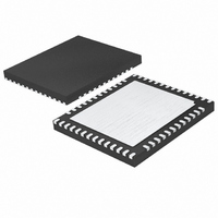
... DRAWING NOT TO SCALE 3. ALL DIMENSIONS ARE IN MILLIMETERS Information furnished by Linear Technology Corporation is believed to be accurate and reliable. However, no responsibility is assumed for its use. Linear Technology Corporation makes no representa- tion that the interconnection of its circuits as described herein will not infringe on existing patent rights. LTC2174-14/LTC2173-14 UKG Package 52-Lead Plastic QFN (7mm × ...
Page 32
... QFN-20 Dual Matched 2nd Order Lowpass Filters with Differential Drivers, Pin-Programmable Gain, 6mm × 3mm DFN-22 Integrated High Speed ADC, Passive Filters and Fixed Gain Differential Amplifi ers www.linear.com ● 21754314f LT 1009 • PRINTED IN USA © LINEAR TECHNOLOGY CORPORATION 2009 ...