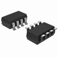
AD7999YRJZ-1500RL7 Analog Devices Inc, AD7999YRJZ-1500RL7 Datasheet - Page 4

AD7999YRJZ-1500RL7
Manufacturer Part Number
AD7999YRJZ-1500RL7
Description
IC ADC 8BIT 4CH SAR I2C SOT23-8
Manufacturer
Analog Devices Inc
Specifications of AD7999YRJZ-1500RL7
Data Interface
I²C, Serial
Design Resources
Using AD8599 as an Ultralow Distortion Driver for the AD7999 (CN0045)
Number Of Bits
8
Sampling Rate (per Second)
1M
Number Of Converters
1
Power Dissipation (max)
4.68mW
Voltage Supply Source
Single Supply
Operating Temperature
-40°C ~ 125°C
Mounting Type
Surface Mount
Package / Case
SOT-23-8
Resolution (bits)
8bit
Input Channel Type
Single Ended
Supply Voltage Range - Analogue
2.7V To 5.5V
Supply Current
850µA
No. Of Pins
8
Operating Temperature Range
-40°C To
Sampling Rate
140kSPS
Digital Ic Case Style
SOT-23
Rohs Compliant
Yes
Lead Free Status / RoHS Status
Lead free / RoHS Compliant
Other names
AD7999YRJZ-1500RL7TR
Available stocks
Company
Part Number
Manufacturer
Quantity
Price
Company:
Part Number:
AD7999YRJZ-1500RL7
Manufacturer:
ADI
Quantity:
3 000
Part Number:
AD7999YRJZ-1500RL7
Manufacturer:
ADI/亚德诺
Quantity:
20 000
AD7991/AD7995/AD7999
Parameter
LOGIC INPUTS (SDA, SCL)
LOGIC OUTPUTS (OPEN DRAIN)
THROUGHPUT RATE
POWER REQUIREMENTS
1
2
3
4
5
6
7
Functional from V
Sample delay and bit trial delay enabled, t
For f
See the Terminology section.
For f
Guaranteed by initial characterization.
See the Reading from the AD7991/AD7995/AD7999 section.
Input High Voltage, V
Input Low Voltage, V
Input Leakage Current, I
Input Capacitance, C
Input Hysteresis, V
Output Low Voltage, V
Floating-State Leakage Current
Floating-State Output Capacitance
Output Coding
V
I
Power Dissipation
DD
DD
SCL
SCL
ADC Operating, Interface Active
Power-Down, Interface Active
Power-Down, Interface Inactive
ADC Operating, Interface Active
Power-Down, Interface Active
Power-Down, Interface Inactive
up to 400 kHz, clock stretching is not implemented. Above f
≤ 1.7 MHz, clock stretching is not implemented; for f
(Fully Operational)
(Fully Operational)
DD
= 2.35 V.
HYST
INL
IN
INH
2
6
OL
IN
7
7
1
7
7
= t
6
2
= 0.5/f
SCL
Min
0.7 (V
0.9 (V
0.1 (V
2.7
.
SCL
DD
DD
DD
> 1.7 MHz, clock stretching is implemented.
Straight (natural) binary
)
)
)
SCL
= 400 kHz, clock stretching is implemented.
Typ
Y Version
Rev. B | Page 4 of 28
18 × (1/f
Max
0.3 (V
0.1 (V
±1
10
0.4
0.6
±1
10
17.5 × (1/f
+ 2 μs
5.5
0.09/0.25
0.25/0.8
0.07/0.16
0.26/0.85
1/1.6
0.3/1.38
0.83/4.4
0.24/0.88
0.86/4.68
3.3/8.8
DD
DD
)
)
SCL
SCL
)
)
Unit
V
V
V
V
μA
pF
V
V
V
μA
pF
V
mA
mA
mA
mA
μA
mW
mW
mW
mW
μW
Test Conditions/Comments
V
V
V
V
V
I
I
f
section
f
section
V
clock stretching is implemented
Digital inputs = 0 V or V
V
V
V
V
V
V
V
V
V
V
SINK
SINK
SCL
SCL
DD
DD
DD
DD
IN
REF
DD
DD
DD
DD
DD
DD
DD
DD
DD
DD
= 0 V or V
≤ 1.7 MHz; see the Serial Interface
> 1.7 MHz; see the Serial Interface
= 2.7 V to 5.5 V
= 2.35 V to 2.7 V
= 2.7 V to 5.5 V
= 2.35 V to 2.7 V
= 3.3 V/5.5 V, 400 kHz f
= 3.3 V/5.5 V, 3.4 MHz f
= 3.3 V/5.5 V, 400 kHz f
= 3.3 V/5.5 V, 3.4 MHz f
= 3.3 V/5.5 V
= 3.3 V/5.5 V, 400 kHz f
= 3.3 V/5.5 V, 3.4 MHz f
= 3.3 V/5.5 V, 400 kHz f
= 3.3 V/5.5 V, 3.4 MHz f
= 3.3 V/5.5 V
= 3 mA
= 6 mA
= V
DD
; for f
DD
SCL
= 3.4 MHz,
DD
SCL
SCL
SCL
SCL
SCL
SCL
SCL
SCL


