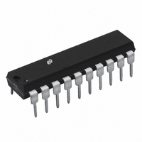
ADC0838CCN/NOPB National Semiconductor, ADC0838CCN/NOPB Datasheet - Page 16

ADC0838CCN/NOPB
Manufacturer Part Number
ADC0838CCN/NOPB
Description
IC ADC 8BIT SERIAL I/O 20-DIP
Manufacturer
National Semiconductor
Datasheet
1.ADC0831CCWMNOPB.pdf
(33 pages)
Specifications of ADC0838CCN/NOPB
Number Of Bits
8
Sampling Rate (per Second)
31k
Data Interface
NSC MICROWIRE™, Serial
Number Of Converters
1
Power Dissipation (max)
15mW
Voltage Supply Source
Single Supply
Operating Temperature
0°C ~ 70°C
Mounting Type
Through Hole
Package / Case
20-DIP (0.300", 7.62mm)
Lead Free Status / RoHS Status
Lead free / RoHS Compliant
Other names
*ADC0838CCN
*ADC0838CCN/NOPB
ADC0838
ADC0838CCN
*ADC0838CCN/NOPB
ADC0838
ADC0838CCN
www.national.com
Functional Description
3. On each rising edge of the clock the status of the data in
(DI) line is clocked into the MUX address shift register. The
start bit is the first logic “1” that appears on this line (all
leading zeros are ignored). Following the start bit the con-
verter expects the next 2 to 4 bits to be the MUX assignment
word.
4. When the start bit has been shifted into the start location
of the MUX register, the input channel has been assigned
and a conversion is about to begin. An interval of
period (where nothing happens) is automatically inserted to
allow the selected MUX channel to settle. The SAR status
line goes high at this time to signal that a conversion is now
in progress and the DI line is disabled (it no longer accepts
data).
5. The data out (DO) line now comes out of TRI-STATE and
provides a leading zero for this one clock period of MUX
settling time.
6. When the conversion begins, the output of the SAR
comparator, which indicates whether the analog input is
greater than (high) or less than (low) each successive volt-
age from the internal resistor ladder, appears at the DO line
8 Single-Ended
4 Differential
FIGURE 1. Analog Input Multiplexer Options for the ADC0838
00558353
00558355
(Continued)
1
⁄
2
clock
16
on each falling edge of the clock. This data is the result of the
conversion being shifted out (with the MSB coming first) and
can be read by the processor immediately.
7. After 8 clock periods the conversion is completed. The
SAR status line returns low to indicate this
later.
8. If the programmer prefers, the data can be provided in an
LSB first format [this makes use of the shift enable (SE)
control line]. All 8 bits of the result are stored in an output
shift register. On devices which do not include the SE control
line, the data, LSB first, is automatically shifted out the DO
line, after the MSB first data stream. The DO line then goes
low and stays low until CS is returned high. On the ADC0838
the SE line is brought out and if held high, the value of the
LSB remains valid on the DO line. When SE is forced low,
the data is then clocked out LSB first. The ADC0831 is an
exception in that its data is only output in MSB first format.
9. All internal registers are cleared when the CS line is high.
If another conversion is desired, CS must make a high to low
transition followed by address information.
The DI and DO lines can be tied together and controlled
through a bidirectional processor I/O bit with one wire. This is
8 Pseudo-Differential
Mixed Mode
00558356
00558354
1
⁄
2
clock cycle


