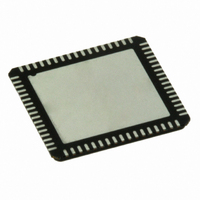
ADC16DV160CILQ/NOPB National Semiconductor, ADC16DV160CILQ/NOPB Datasheet - Page 25

ADC16DV160CILQ/NOPB
Manufacturer Part Number
ADC16DV160CILQ/NOPB
Description
ADC 16BIT DUAL 160MSPS 68LLP
Manufacturer
National Semiconductor
Series
PowerWise®r
Datasheet
1.ADC16DV160CILQNOPB.pdf
(30 pages)
Specifications of ADC16DV160CILQ/NOPB
Number Of Bits
16
Sampling Rate (per Second)
160M
Data Interface
Serial, SPI™
Number Of Converters
2
Power Dissipation (max)
1.47W
Voltage Supply Source
Single Supply
Operating Temperature
-40°C ~ 85°C
Mounting Type
Surface Mount
Package / Case
68-VFQFN, Exposed Pad
Leaded Process Compatible
Yes
Rohs Compliant
Yes
Peak Reflow Compatible (260 C)
Yes
Lead Free Status / RoHS Status
Lead free / RoHS Compliant
Other names
ADC16DV160CILQ
Register Map
Note: Accessing unspecified addresses may cause functional failure or damage. All reserved bits must be written with the listed
default values.
Operation Mode
DF
Bit 7
Bits (6:5)
Bit 4
Bit 3
Bit 2
Bit 1
Bit 0
Synchronization Mode
Bit 7
Bit 6
Bit 5
Bits (4:2)
Bit 1
Bit 0
Sample
Phase
7
7
Operation Mode
Data Format
Operation Mode
0
0
1
1
Reserved. Must be set to 0.
Reserved. Must be set to 0.
Reserved. Must be set to 1.
Full scale. Full scale can be adjusted from 2.0 to 2.4V
Restore Default Register Values. Default values of SPI registers can be restored at the rising edge of this bit.
Sampling Clock Phase. This is for synchronizing sampling edge for multiple devices while the ADC16DV160 is
configured at clock divide by 2.
Clock divider. Internal operating clock frequency can be programmed either to be divided by 1 or 2.
Reserved. Must be set to 0.
Output Clock Phase Adjustment. User can adjust output clock phase from 31° to 143°. Each 1 LSB increment
results in about 16° of output clock phase increase.
0
0
0
0
1
1
1
1
Reserved. Must be set to 0.
Reserved. Must be set to 0.
Clock Divider
6
6
0 Keep sampling edge as is (default).
1 Invert internal clock to adjust sampling edge.
0 Divide by 1 (default).
1 Divide by 2
1
0
0
1
0
1
0
1
1
0
0
0
1
1
0
0
1
1
Reserved
5
5
Two's Complement
Offset Binary (Default)
Normal Operation (Default)
Sleep Mode. Device is powered down, but it can wake up quickly.
Power down mode. Device is powered down at lowest power dissipation.
Fixed pattern mode. Device outputs fixed patterns to check connectivity with interfacing
components.
2.0V
2.4V
Restore default register values
As is (default)
Reserved
0
1
0
1
0
1
0
1
PP
PP
4
(default)
4
Output Clock Phase
95° (default)
Addr: 01h
111°
127°
143°
31°
47°
63°
79°
25
Addr: 00h
3
3
PP
.
Full Scale
2
2
Reserved
1
1
Default
Reserved
www.national.com
0
0
R/W
R/W


